|
April 20,
2003
Looking at Intel's Prescott
die, part II
(
by Hans de Vries )
|
Article
Index
 Yamhill
comes out of the "blue" Yamhill
comes out of the "blue"
Code names of 64 bit enabled processors and chipsets.
Our detailed overview of Intel's Pentium 5 / Pentium
6 processor.
Our detailed overview of Intel's Pentium 4 processor.
Improvements
found so far
The
need for 64 bit processing: Closer than you think.
The
Second
integer core is for 64 bit processing (not for multithreading)
No
double frequency building blocks used yet.
48
bit virtual addresses: The Instruction TLB
48
bit virtual addresses: The virtual Trace Cache tags
48
bit virtual addresses: The Front End and Trace Cache Branch Target
Buffers
Re-examining
the Register Alias History Table: 128 uOps in flight in
total.
Faster
SSE Floating Point separated from legacy Floating Point.
La
Grande: A tiny embedded processor for (micro)-code decryption and
other purposes?
|
|
Yamhill
comes out of the "blue"
Googlers: This article looks for Yamhill in
Prescott's.
If you are looking
for Prescott's in Yamhill
go here
:
http://www.prescottbluebird.com/portland.html
We've found lots of prove for 64 bit processing
now in Prescott's blue
die image. Yamhill is for sure. That's what we can say. Virtual Addressing
has been extended from 32 bit to 48 bit just like in the AMD Hammer family. We
will demonstrate it with illustrated images of three different locations: The
instruction TLB, The Trace Cache and the Front End Branch
Target Buffers. Other examples of increased address space are scattered all over
the chip. The processor however won't be called Prescott or Nocona anymore when
the 64 bit features are enabled. New code names are used for 64 bit
enabled processors. The later two will stay with a 32 bit virtual address
space but have their physical address space already extended from 36 to 40
bit as seems to be mentioned in manuals still under NDA.
|
|
Code names of 64 bit enabled processors and chipsets
The name that appeared for the
64-bit-enabled, 4P- server version is Potomac. A processor matched to
the Twin Castle server chipset scheduled to hit the market in the second
half of 2004. A new code name recently appeared, Jayhawk, as being
the dual processor version which is matched with the Lindenhorst chipset
slated for the beginning of 2005. Furthermore, The name of a desktop and
workstation chipset has appeared: Copper River, coupled with an
unnamed processor coming after Prescott but before Tejas. The
Copper River chip-set is planned to arrive at the second half of 2004,
more or less at the same time as Potomac and Twin castle. The only thing
missing now is the code name for this 64 bit desktop version. Or.... maybe
its name was Yamhill in the first place? Well... would be difficult to
put that one on a roadmap now and then still deny 64 bit :^)
It
seems that the processors come in generations. So Prescott and Nocona would
be Pentium 5's while Potomac, Jayhawk and "Yamhill" could be
Pentium 6's Then, as generally expected, The Tejas line as Pentium 7's
and the Nehalem's as Pentium 8's
|
|
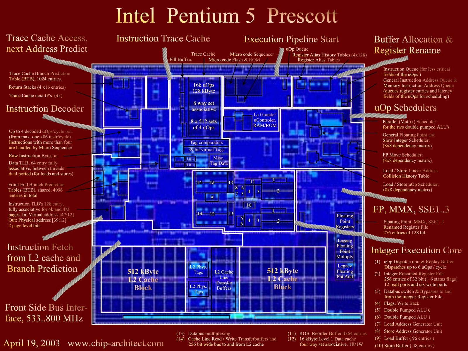
Only
on Chip-Architect:
Our detailed overview of Intel's Pentium 5 / Pentium
6 processor. version 1.0
Instructions
run clockwise. Click here
for a large
version (1600x1200)
|
|
|
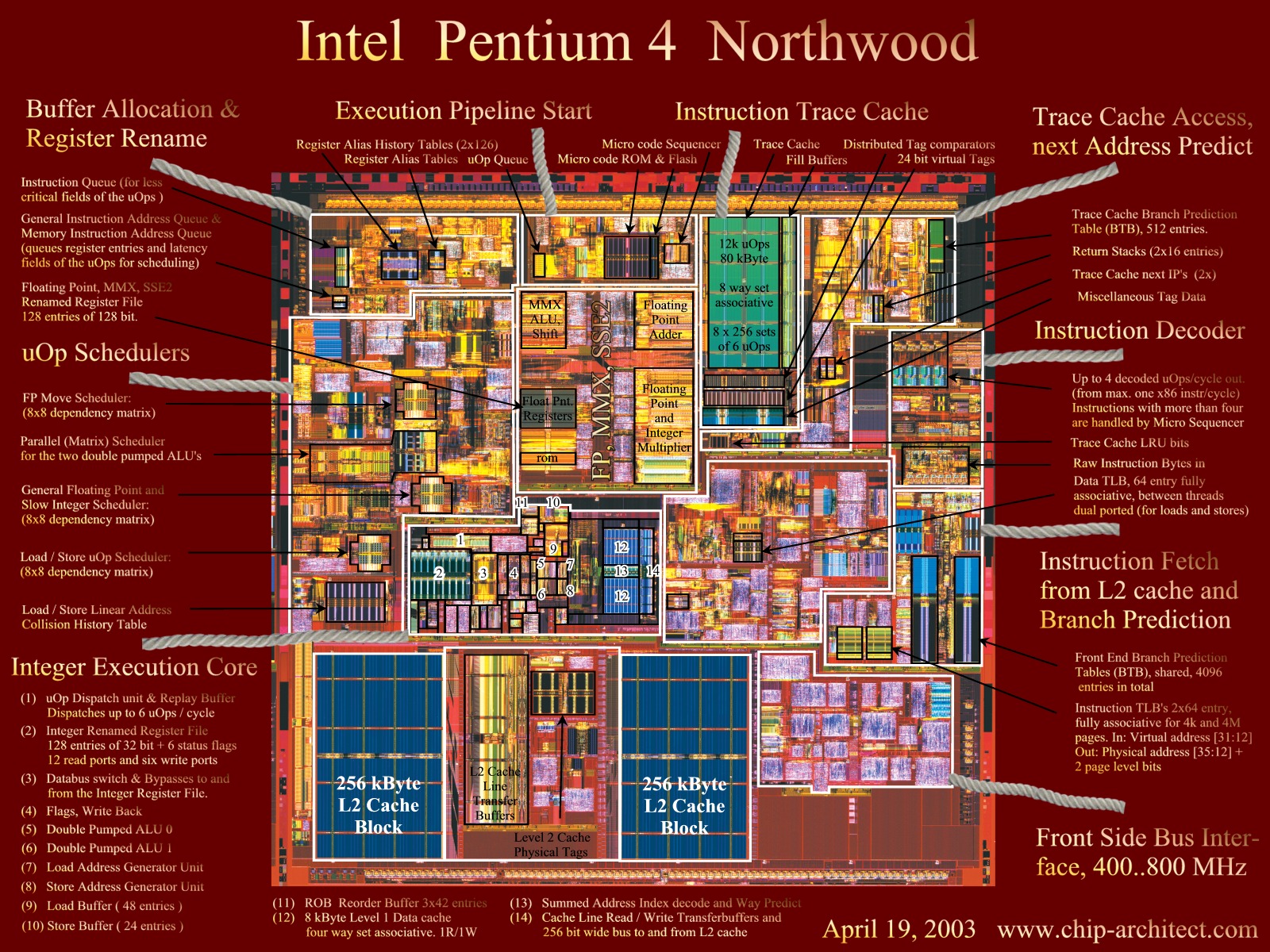
To compare:
Our detailed overview of Intel's Pentium 4 processor.
version 1.0
Instructions
run counter-clockwise. Click here
for a
large (1600x1200) and here
for a huge version (3200 x 2400)
|
|
The
need for 64 bit processing: Closer than you think.
64
bit virtual addressing for the desktop will be needed many years before
4 GByte physical memory becomes common place on your motherboard . The
point is that the whole idea of virtual memory with page management only
works if the virtual memory space is much larger then your physical
memory. I actually had to save my work and restart the image software many
times during the work on the large images of this article, edited
in uncompressed mode. Often I had to shoot down by hand as many tasks possible with Task Manager to
free virtual memory just to get my work saved. The
problem is not the 1 Gigabyte DDR on my Dell Inspiron 8200. The whole
problem is the 4 Gigabyte virtual memory limitation which becomes so polluted with scattered around bits and pieces of allocated memory so
that it's not possible to find a decent part of continues memory
anymore. All the result of course of languages like C with explicit
pointer handling and processors that do not have specific pointer
registers. There is no way to defragment virtual memory like a hard disc
to open up larger continuous areas. The only way to "defragment"
virtual memory is to save your
work on time, shut down the program and restart again.I think these
mission critical 32 bit bank transaction servers only work because they
start up and kill small processes all the time to avoid virtual memory
pollution. Imagine that you have to start killing all kinds of
tasks by hand in the hope that you can save a few hours worth of bank
transactions....
|
Second
integer core for 64 bit processing (not for multithreading)
It
is as good as sure that the second 32 bit core is exclusively used
for 64
bit processing, and in a way similar to the good old bit slices. There
was the 4-bit AMD 2901 that could be used to build 16, 32 or 64
bit processors. The fact that makes it possible is because the core's is
limited mainly to additive and logic functions. A 64 bit staggered
addition will take a total of four 1/2 cycles but you can start two of
them back to back on 1/2 cycle intervals. The latency to access the
cache also does not need to be increased because of the extension to 64
(48) bit addresses. The higher part of the address is only used several
cycles later to check the address tags with the TLB entries and not to access the data cache
itself. What will increase with one cycle is the latency from an ALU
instruction to a normal speed integer instructions. This delay will
increase from 2 to 3 cycles. One extra pipeline stage is needed as well,
resulting in a minor increase in the branch miss prediction penalty.
The
reason that we can be so sure that the second core is not
used to boost the 32 bit Hyper threading capabilities is the scheduler.
This unit is by far the biggest entity on the Pentium 4 die. It is
larger then all the Floating Point, MMX and SSE hardware together. It is
not only big but it also consist mostly out of very timing critical
optimized macro cells laid out by hand. It takes a lot of time and
effort to change the scheduler. We've looked to it in detail and
concluded that it has mainly remained unchanged on Prescott's die. This
means that the maximum uOp throughput remains six per cycle using the
same dispatch ports as the Pentium 4.
|
No
double frequency building blocks used yet
We found that none of those fancy very
high performance building blocks demonstrated during the VLSI 2002
conference are used in Prescott. They will have to wait for a Prescott
successor. The scheduler needs to be modified to support them. Some
of these building block are very impressive indeed. The 32kByte cache
block shown may for instance be used to implement something like a 128
kByte L1 cache with 2 read operations per 1/2 cycle, all within the same
load latency as the current Pentiums 4. So: 16 times the size (128k/8k)
and four times the number of reads!
|
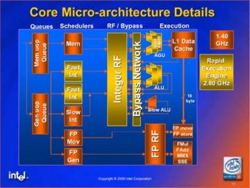
It
is now clear that both the schedulers for the Rapid Execution
Engine and the Integer Register File do not operate at the
double frequency like it is suggested in an Intel presentation
from 2000 shown at the right here.
These
units do fully support the double pumped ALU's but they do so by
doing things in parallel and not by operating at a double
frequency. Now this is of course OK, but a number of articles I
wrote based on this just don't make much sense. Such as in my
first Prescott article
from a year ago where I said that a 4GHz Prescott equipped with
a double speed Data Cache should be called an 8 GHz
processor..... |
There's
to much yellow in here! |
Now
when will we see building blocks used like the ones that were
demonstrated during the VLSI 2002 conference? The only future frequency
roadmap for Tejas and Nehalem we saw came from Mike Magee's, The
Inquirer here.
"
The immediate successor to Prescott after it tops out at 5.20GHz will be the "Tejas" core, also produced on a 90 nanometer process and delivering 5.60GHz using a 1066MHz system bus. That's slated to start appearing towards the end of 2004.
Tejas will increase in steady increments which appear to be 6GHz, 6.40GHz, 6.80GHz, 7.20GHz, 7.60GHz, 7GHz, 8.40GHz, 8.80GHz and topping out at 9.20GHz.
The first Nehalem is supposed to appear at 9.60GHz before Intel succeeds in its goal to produce a 10GHz+ chip, the Nehalem, and using a 1200MHz front side
bus. "
Interesting
is also the paper
"Increasing
Processor Performance by Implementing Deeper Pipelines"
from Intel's Eric Sprangle and Doug Carmean. The paper looks at a theoretical
double frequency version of the current Pentium 4. Both now work on the
Nehalem with Doug as it's principle architect. They maintain that the
study should not be interpreted like a roadmap document.
|
|
Improvements
found so far
A
list of improvements we found out on the Prescott/Nocona/Yamhill/Jayhawk/Potomac die until now.
Only
few of them are officially disclosed by Intel. (
so it's all unofficial )
|
|
|
Specifications
and
Enabled
Features
|
Pentium
4
(
current )
Northwood,
SP
Prestonia,
DP
Gallatin,
MP |
Pentium
5
(
Q4 - 2003 )
Prescott,
SP
Nocona
, DP
|
Pentium
6?
(
H2 - 2004 )
"
Yamhill ", SP
Jayhawk,
DP
Potomac,
MP
|
|
Data
Width |
32
bit |
32 bit |
64
bit |
|
Virtual
Address
Physical
Address |
32
bit
36
bit |
32
bit
40
bit |
48
bit
40
bit |
|
Architectural
Registers |
8 |
8 |
16? |
|
Logical
Processors
(number
of threads) |
Northwood:
1,2
Prestonia:
2
|
Prescott:
2
Nocona:
4?
|
Jayhawk:
4
Potomac:
4 |
|
Frequency
and
estimated
Spec
Int 2000 |
up
to 3.2 GHz
1250 |
start
at 3.4 GHz
1500 |
start
at 4.0 GHz?
1900
(16 regs ) |
|
Chipsets:
Desktop
Processor
Server
Single Processor
Workst.
Dual Processor
Server
Dual Processor
Server
Four Processor |
Canterwood
Brookdale
Placer
533
Plumas
533
- |
Canterwood
Canterwood
ES
Placer
533, Tumwater
Plumas
533, Lindenhorst
- |
Copper
River
Copper
River
Tumwater
Lindenhorst
Twin
Castle |
|
ALU
Throughput (max)
|
four
32 bit ops/cycle |
four
32 bit ops/cycle |
four
64 bit ops/cycle |
|
ALU
Latencies:
ALU to ALU instruction
ALU to Cache adddress
ALU to Other Instruction |
1/2
cycle
1/2
cycle (32b)
2
cycles |
1/2
cycle
1/2
cycle (32b)
3
cycles? |
1/2
cycle
1/2
cycle (64b)
3
cycles |
|
L1
Data Cache |
8
kByte |
Prescott
16
kByte
Nocona
16 kByte?
|
32 kByte |
|
L1
Bandwith (Integer)
L1
Data Cache Reads
L1
Data Cache Writes |
one
32 bit word/cycle
one
32 bit word/cycle |
one
32 bit word/cycle
one
32 bit word/cycle |
one
64 bit word/cycle
one
64 bit word/cycle |
|
Instruction
Trace Cache |
12
k uOps / 80 kByte
256
sets
8
ways
6
uOps per trace-line
53
bit per uOp |
16
k uOps / 128 kByte
512
sets
8
ways
4
uOps per trace-line
64
bit per uOp |
16
k uOps / 128 kByte
512
sets
8
ways
4
uOps per trace-line
64
bit per uOp |
|
Trace
Cache Bandwidth |
3
uOps/cycle |
4
uOps/cycle |
4
uOps/cycle |
|
L2
Unified Cache |
512
kByte |
1024
kByte |
1024
kByte |
|
Branch
Prediction:
Trace
Cache BTB
Front
End BTB |
512 entries
4096
entries |
1024
entries
4096
entries |
1024
entries
4096
entries |
|
Instructions
in Flight |
126 |
128 |
128 |
|
Integer
Register File |
128
x 32 bit |
256
x 64 bit |
256
x 64 bit |
|
Floating
Point
Register File
|
128 x 128 bit |
256 x 128 bit |
256 x 128 bit |
| Load Buffer |
48 entries |
96 entries |
96 entries |
|
Store Buffer
|
24 entries
|
48 entries
|
48 entries
|
|
Micro
Code:
Relative
ROM size
Relative
Flash size
secure
encrypted download
|
1.0
X
1.0
X
no? |
2.1
X (0.71 mm2)
4.3
X ( 0.27 mm2)
yes? |
2.1
X (0.71 mm2)
4.3
X (0.27 mm2)
yes? |
(updated
April 18, 2003)
|
|
48
bit virtual addresses: The Instruction TLB
We'll now go after some
proof for 48 bit virtual addressing. Calculations are 64 bit but, like
in the Hammer, only the first 48 bit are used for virtual addressing (
the address as the programmer sees it ) and 40 bits are used for
accessing physical memory (The memory dimms on your
motherboard) As said, the virtual memory address range must
be much larger then the physical in order for paged based memory
management to work. The main reason why 64 bit processors are needed
well before you can afford 4 Gigabyte of memory.
The TLB ( Translation Look
aside Buffer ) is responsible for translating the virtual address into a
physical address. So it's indeed the obvious place to start
looking! The TLB is a little cache that contains recent
translations. If it's not in the TLB then the translation must be loaded
from the memory hierarchy, possible all the way down from main
memory. The TLB's here are fully associative and are thus
basically Contents Addressable Memories. The consist out of two parts.
The upper rectangle holds the latest virtual addresses that were
translated and each stored virtual address has its own comparator that
checks if its equal to the new virtual address that must be translated.
The comparators are organized as columns in
|
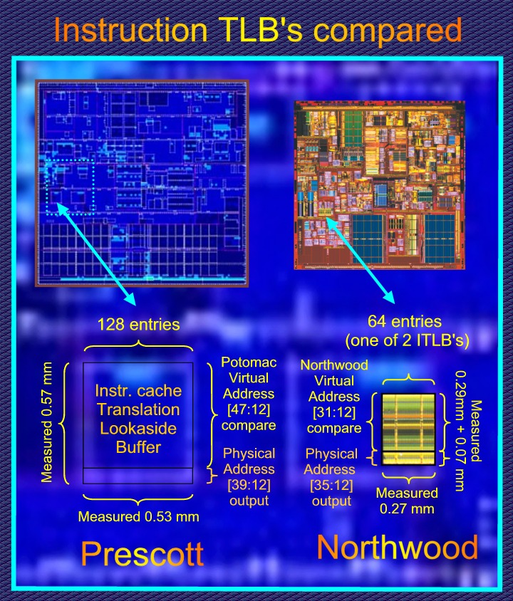
|
|
the
upper rectangle. A stored virtual address that matches will send an
enable signal downwards to the lower rectangle where the physical
addresses are stored. The corresponding physical address is selected and
the translation is complete. We know that the height of the upper
triangle is proportional to the size of the virtual address while the
height of the lower rectangle is proportional to the physical address.
As you can see in the Image above: There is a very good correspondence
with the real size size of Prescott's TLB (vague white rectangle) and
the calculated size, the black one.
Northwood
has two 64 entry TLB's, one for each thread, while Prescott's has
a single 128 entry instruction TLB shared among all threads.
|
48
bit virtual addresses: The virtual tags of the Trace Cache
We've already seen earlier
that Prescott's Trace cache is significantly larger the the one of
Northwood. Knowing the right scaling we can hold the two next to each
other to see the exact difference. We found that the Willamette, Pentium
4 trace cache is build using 20 of the same 4k Byte memory tiles that
were used in the L2 cache of Willamette. This does not only tells us a
lot about the size (80 kByte) but also how it is accessed. The Prescott
Trace Cache is constructed with 8 memory tiles. These tiles have the
same height as Prescott's L2 cache tiles. They are however some 30%
wider
|
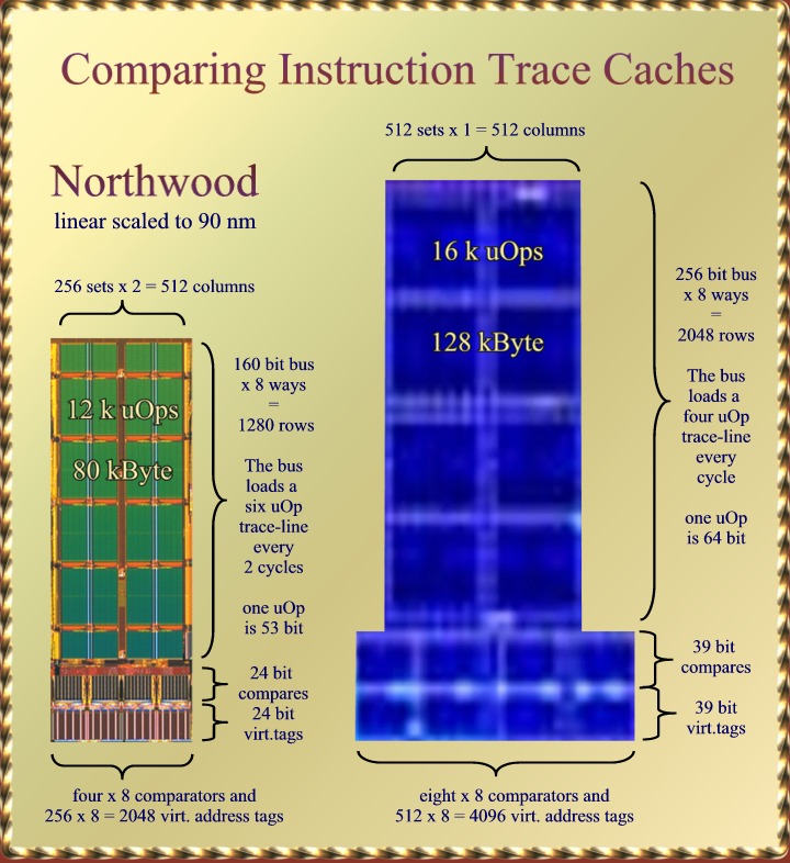
|
because
there are 256 extra word lines running vertically. Northwood's
Trace Cache has a 160 bit bus to read 3 micro operations (uOps) per
cycle, so each uOp has about 53 bits. A single trace has 6 uOps and is
read in two cycles. The
160 bus is build up from thick copper global bit lines that get
information from one of sixteen local bit-lines. Each 6 uOp trace can
come from any of 8 "ways" The number 8 is there because
the Trace Cache is "8 way, set associative" It
works like this: The cache has 256 "sets", This
means that 8 bits from the address are used to select a set from the
cache. Now each set has 8 "ways" Each way remembers the
remaining 24 bit of the instruction address in an "address-
tag" field These tags must be compared with the corresponding 24
bits of the address requested. If one of them fits then we have a
"cache-hit" and the right way is selected to provide the uOps.
Northwood's Trace Cache is constructed from four big columns. In each
column you can see, At the bottom: The storage space for the 24
bit address tags, above that: the eight 24 bit comparators, and above
that you can see the large green column that stores the uOps. We
now go to Prescott's Trace Cache: It's significantly higher which
corresponds to a 256 bit bus, enough for four uOps of 64 bit each, about
5 bits more per uOp are needed to support something like AMD's x86-64.
An issue now arises with the trace-line size. Trace lines with 8 uOps
are less effective because positions in the line after a branch are left
empty, uOps are stored at the begin of a new trace-line instead. It
would be better instead to have trace-lines of only 4 uOps instead.
This has also its advantages for hyper-threading: Instead of needing two
cycle to read out one trace-line we can now read out a new trace line
every cycle and can alternate between threads on a per cycle base. Precott's
Trace Cache becomes "512 set, 8 way associative" as a consequence.
The 512 sets means that the number of address tags must be doubled.
Furthermore, with 48 bit virtual addressing we now need 39 address bits
for the tags. That is: 48 - 9. The remaining 9 bits are used to
select between the 512 sets. We
are reassured by a hint that was dropped to C'Ts Andreas Stiller here
where a "finer" Trace Cache access was reported in order to
better support hyper threading.
|
48
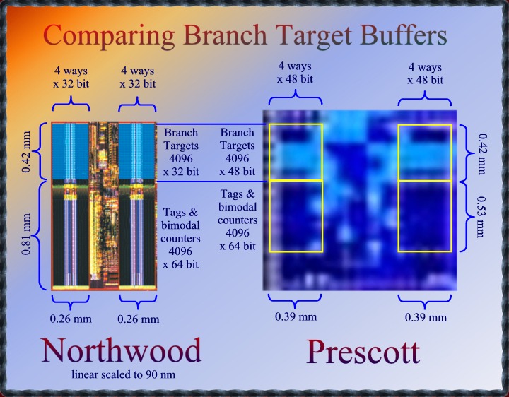
bit virtual addresses: The Front End Branch Target
Buffers
This unit is used for
branch prediction and is located at edge of the L2 unified cache were
the instruction pre-fetcher loads raw instruction bytes that are to be
decoded and then stored as uOps in the instruction trace cache. You can
see two columns that are very similar the single column found on the
Pentium Pro, Pentium II and III. The (smaller) upper rectangle contains
what we want the know: The branch target address. The lower rectangle
contains the address-tags needed to select between the different ways
and to detect cache-hit or cache-miss. It is known that the previous
Pentiums stored the entire 32 bit address as a tag, so also the bits
used to select between the sets, There is no real use for this, except
maybe to detect "entry valid" An entry would be valid if the
extra tag bits are identical to the set they are stored in.
We can see that Prescott's
BTB's are 50% wider which corresponds nicely to the 48 bit addressing.
The lower rectangle in Precott however has almost exactly the same area
as in Northwood. The lower area also contains the prediction
information. Each entry has maintains 16 "bimodal counters" of
2 bit each. The 2 bit values mean: 0=likely not taken, 1=probably not
taken, 2=probably taken, 3=likely taken. The selection between the
sixteen counters is based on the outcome of the four previous times that
the branch was executed. (local branch history)
|
|
|
Now branch prediction is an
imprecise process. Incorrectly predicted branches can always be
corrected. There can be some nasty side effects of erratic branch
prediction however. The whole Trace Cache may be invalidated at once if
it turns out that uOps were decoded from a data memory page which is
shortly thereafter written to. The "self-modifying- code"
detector will sound the alarm and invalidate the entire trace
cache. So, some attention is needed here! We think that some
of the redundant address-tag bits may have been replaced with address
bits from 32 and higher.
So full 48 bit address
targets avoid the "self-modifying-code" issue while a few more
relevant bits in the tags will reduce conflicts between branches to
those "tera-bytes" apart.
|
|
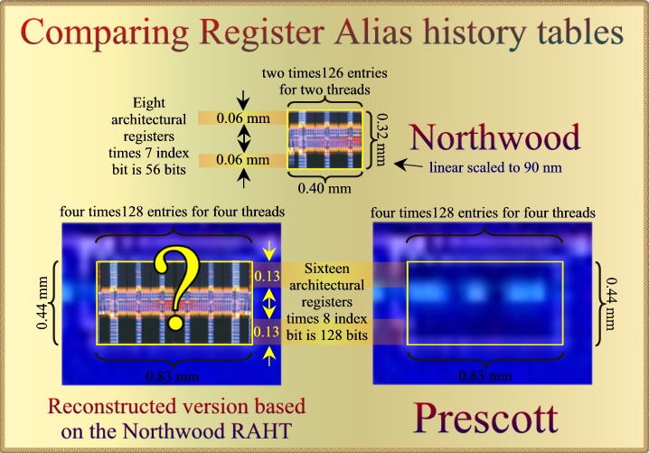
Re-examining
the Register Alias History Table, 128 uOps in flight in total.
We
wrote about the Register Alias History Table before
a while ago were we concluded that the number of in-flight uOps had
doubled in Prescott. This based on the fact the RAHT (Regiser Alias
History Table) more than doubled in size. This table must remember
information for all instructions in-flight so that the processor can go
back in time and discard results from instructions that were erratically
executed because of branch-miss-prediction. There is no absolute need to
store information for more instructions since they will be all be
retired after branch prediction has been checked.
However.
Intel's implementation is such that it maintains a maximum sized table
for each processor thread as one can see in a MPF 2002
presentation. Northwood's RATH thus has 252 entries for two times
126 instructions in flight.
Now
what do we make of the fact that Precott's RAHT has more than
doubled?
|
|
| We do not
expect 256 instructions in-flight since we've concluded that the second
integer core can not execute instructions independently. Four
threads is one way. It would double the RAHT but it would not
"more-than-double" it. The second options has to do with it's
contents. It remembers the mapping for each of the eight architectural
registers into the 128 entry Register Files. An increase of the number
of architectural registers from 8 to 16 would result in twice the
storage needed. We may need 8 index bits because the Register Files have
increased from 128 to 256 entries.
The Image above details an
and-and implementation. Closer scrutiny of the Northwood RAHT shows that
the actual storage areas are only a fraction of the total size. The
black rectangles. The rest of the area may be bypasses. New registers
indices are produces for 3 uOps per cycle in the Northwood and 4 uOps in
Prescott. The last uOp, number 3 or 4 is dependent on the other ones.
The data-busses run horizontal so the height of the black rectangles is
proportional to the amount of data per entry. The above implementation
example provides a "perfect fit" but you can always find
perfect fits in more complicated cases like this one.
Still, we rate the chances
for an "and-and" implementation the highest. So, four threads
and 16 architectural registers. Are four threads useful in
Prescott? Given that the maximum uOp dispatch rate is still 6 uOps
per cycle? I think certainly yes in server implementations.
Latency from main memory is the reason. A thread may need to wait
hundreds of cycles for data from main memory. Prescott has all out of
order buffers doubled to support two threads. If one thread is waiting
for main memory then the other can run unlimited just as fast as a
single thread would. I can imagine that in a 4P server with a shared
data bus will see latencies to memory much longer with a significant
chance that both threads are waiting hundreds of cycles for data from
the non-distributed memory. Two extra threads may fill up some of these
lost cycles.
|
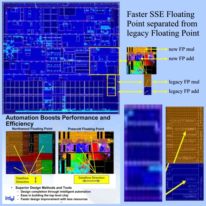
Faster
SSE Floating Point separated from legacy Floating Point
The
Pentium 4 handles all multiplies with a single unit. The legacy x87, The
integer, The MMX and the SSE ones. This results in longer latency times
for integer multiplies and SSE floating point multiplies that use the
hardware of the 80 bit x87 multiplier. We've shown in a previous article
that the unit that handles all Floating Point, MMX and SSE instructions
has moved to a different location on the die ( To make room for new
undisclosed hardware? )
|
|
|
You
can see the new location in the illustration above. What not was
disclosed was that this unit has a "tail". Somewhat to our surprise
we found that the macro-cells in this area are identical to the Floating
Point adder and the Floating Point Multiplier (minus MMX multiply)
The "Prescott Floating Point" hardware is supposed to be
allocated in the rectangle showed! Now what has happened here? It
seems that the older legacy FP hardware has now been isolated to be able
to design faster SSE2 floating point units not hindered by legacy
hardware anymore. This also results in lower inter multiply latencies as
already disclosed by Intel.
|
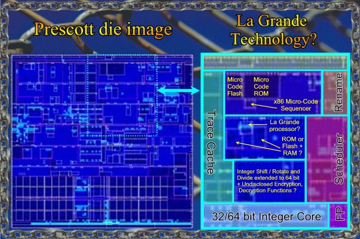
La
Grande: A tiny embedded processor for micro-code decryption and
other purposes?
Maybe
I'm fooling myself, After all, what led me to the ideas below was an
Intel patent granted on April 1st, 2003 !
US
patent 6549821. Not an Oregon patent however, but la Grande is to be
supported by all processors. It talks among other things about downloading encrypted
micro code for security reasons. This
would need a little decryption engine next to the micro-code instruction
sequencer. The patent also mentions how downloaded micro-code could
enable undisclosed processor functions. In fact it can also change the
x86 instruction codes for these functions every time so that what seems
to be just random data may actually be an executable x86 program that
works until the next time that the micro code is changed. It soon
started to appear to me that this could be the way to realize a lot of
those vague ideas hanging around the announced ( but never explained )
La Grande security technology. And yes, the amount of Micro-code
flash memory has more then quadrupled on the Prescott as compared to the
Pentium 4, and the Micro Code ROM has been doubled. All indications that
something may be going on there. And yes there are these three closely
coupled and partly overlapping macro-cells that look just like the
classical uP /ROM /RAM trinity. All within a space of less then a square
mm.
|
|
|
It's
surrounded by an area which has been puzzling to us because it was left
over after all known Pentium 4 functionality was accounted for on other
locations. The Floating Point unit was moved from here to another
location on the die. It does look like the Micro Code Sequencer ( A tiny processor by itself ) has
had a little brother. They would be sitting just 400 um apart. The La
Grande processor would measure no more then 320 um by 360 um compared to
260 um by 300 um for the even smaller Micro Sequencer. Something
what seems to be part of La Grande is the option to allocate a protected
area in the level 2 cache. Encrypted instructions must be securely
decrypted and stored as executable instructions in the L2 cache. Such
may be another job for a little encryption engine. It's all highly
speculative of course. Speculations that comes partly from the fact that
the Floating Point hardware was moved away from this area and not
replaced with other known hardware, so something new must be there..
|
|
Regards,
Hans
|
|
Related
articles
March
6, 2003: Looking
at Intel's Prescott die, part I
March
26, 2003: Clues
for Yamhill
|
|