|
Chapter
2, Opteron's
Floating Point Units
|
|
|
|
|
|
2.1 The
Floating Point Renamed Register File
|
|
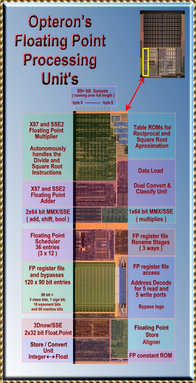
Opteron's
Floating Point renamed register file has been
increased from 88 to 120 entries. It is
a renamed register file in the classical
meaning of the word. It's a single entity that
must contain all architectural
(non-speculative) and speculative values for
the registers defined by the instruction
set.
The
Opteron restores the support for 72
speculative instructions again. The support
for speculative instructions was decreased
from 72 to 56 with the introduction of the
Athlon XP core that included the eight 128 bit
XMM registers for SSE but did not increase the
size of the 88 entry renamed register file.
Each 128
bit XMM register uses two entries in the
renamed register file. The Opteron thus uses
32 entries to hold the architectural (retired)
state of the now 16 XMM registers, which
explains the increase: 88 + 32 makes 120
entries.
40 of the
120 entries are used to hold the architectural
(non-speculative) state of the registers
defined by the instruction set. 32 are
used for the sixteen XMM registers. 8 are used
for the eight x87/MMX registers.
A further
8 register entries are used for micro code
scratch registers, some- times called
micro-architectural registers. These registers
are not defined by the instruction set and are
not directly visible to the programmer. They
are used by micro code to calculate complex
floating point calculations like sine or log
instructions.
The
48 (40+8) entries that define the
architectural state of the processor are
defined by the 48 entry Architectural
Tag Array. The entries that hold
the very latest speculative values
for the 48 architectural register entries are
identified with the 48 entry Future
File Tag Array.
The
speculative state of the processor needs to be
discarded in case of a branch-miss-prediction
or exception. This is handled by overwriting
the 48 entries of the Future
File Tag Array with those of the Architectural
Tag Array.
Each entry
of the renamed register file is 90 bit wide.
Floating Point Values are expanded to a total
of 90 bits (68 mantisse, 18 exponent, 1 sign
bit and 3 class bits) The three class bits
contain extra information about the floating
point number. The class bits also identify non
floating point numbers (integers) which are
not expanded when written in the renamed
register file.
|
|
|
The 120
registers
|
|
8
32
8
|
non speculative registers:
FP/MMX registers
(arch.)
SSE/SSE2 registers
(arch.)
Micro Code Scratch
registers (arch)
|
|
8
32
8
24
|
speculative registers
FP/MMX registers (
latest )
SSE/SSE2 registers
( latest )
Micro Code Scratch
reg. (latest )
Remaining
speculative
|
|
|
The 90
bit registers
|
|
68
18
1
3
|
subdivision of the 90 bits
for FP
Mantisse bits
Exponent bits
Sign bit
Class Code bits
|
|
|
Definition of
the 3 bit Class Code
|
|
0
1
2
3
4
5
6
7
|
Zero
Infinity
Quit
NAN (Not A Number)
Signaling
NAN (Not A Number)
Denormal (very small
FP number )
MMX / XMM (non FP
contents)
Normal ( FP
number, not very small )
Unsupported
|
|
|
|
|
|
|
|
|
|
|
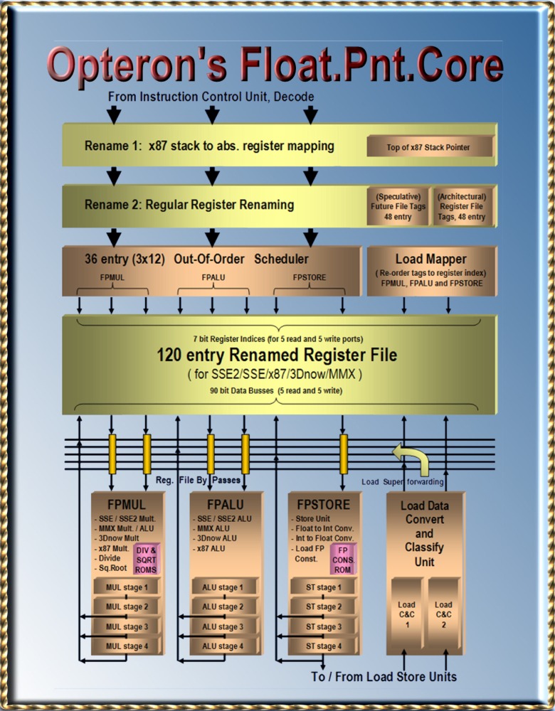
2.2 Floating
Point rename stage
1: x87 stack to absolute
FP register mapping
|
|
The "stack
features" of the legacy x87 are undone in this
first stage of the Floating Point
pipeline. The x87 instructions access
the eight architectural 80 bit registers via a
3 bit Top Of Stack (TOS) pointer. Instructions
use the TOS as both source and destination.
The second argument can be another value on
the stack relative to the TOS register or a
memory operand. The 3 bit TOS pointer is
maintained in the 16 bit x87 FP status
register.
The x87
TOS register relative references are replaced
by absolute references which directly identify
the x87 registers involved in the operation. A
speculative version of the TOS pointer is used
for the translations. The 3 bit pointer can be
updated by the actions of up to three
instructions per cycle. Instructions
can be speculative but are still in order at
this stage. They've not yet been scheduled by
the Floating Point Out-Of-Order scheduler.
If an
exception or a branch-miss-prediction occurs
then the speculative TOS pointer is replaced
with the non-speculative retired one which is
retrieved from the reorder
buffer. The retired version reflects the
value of the TOS during the instruction just
prior to the one that caused the exception or
branch miss prediction.
|
|
2.3 Floating
Point rename stage
2: Regular Register
Renaming
|
|
The actual
register renaming takes place in this stage.
Each instruction that needs a destination
register gets one assigned here. The
destination registers must be unique in
respect to all other instructions in flight.
No instructions may write to the same
register.
Up to
three free register entries are obtained from
the register free list. There are 120
registers available in total. The free-list
can have a maximum of 72 free entries, equal
to the maximum number of instructions in
flight.
The
remaining 48 entries hold the values of the
(non-speculative) architectural registers: The
eight x87/MMX registers, The eight scratch
register (accessible by micro code only)
and the sixteen 128 bit XMM registers for SSE
and SSE2, each using two entries. These
registers are not at a fixed location but may
occupy any of the 120 entries. This is what
makes the free-list necessary. The 48
entries occupied by the architectural
registers mentioned above are identified by
the 48 entry Architectural
Tag Array. It has an
entry for each architectural register with a
value that points to one of the 120 renamed
registers.
Up to
three instructions can thus be renamed per
cycle. The data dependencies are handled with
the aid of another structure,
the 48
entry Future File Tag Array
This array contains pointers the 48 renamed
registers that contain the very latest
speculative values for each of the
architectural registers. The
instructions that are getting renamed access
this structure to obtain the renamed registers
were they can find their source operands. The
instructions will then store the renamed
register which was allocated to them to the Future
File Tag Array so that subsequent
instructions know were to find the result
data.
Example:
An instruction uses architectural registers 3
and 5 as input data and writes its result back
into register 3. It will first read entries 3
and 5 to obtained the pointers to the renamed
registers that contain or will contain the
latest values for register 3 and 5.
Say renamed
registers 93 and 12. The
instruction now knows its source registers, 93
and 12 and can overwrite entry 3 of the Future
File Tag Array with the renamed register
it was assigned to store it's result, say 97.
A subsequent instruction that needs
architectural register 3 will now use renamed
register 97.
If an
exception or branch-miss-prediction occurs
then the 48 entries of the Future
File Tag Array are overwritten with the
48 entries from the
Architectural Tag Array. All
speculative results are thereby discarded. The
pointers in the Architectural Tag Array were
written there by the retirement logic. Up to
three values can be written per cycle for each
line of instructions that retires. The values
are taken from the Reorder
Buffer. The Reorder Buffer is shared by all
instructions.
Floating
Point Instructions that finish write certain
information like exception status, TOS used
et-cetera into the Reorder Buffer. This
information includes also the destination
register they modify, Both the number of
to the architectural register and the renamed
register are stored in the Reorder
Buffer. The two of them are used to
update the Architectural Tag Array at
retirement. One as the data and the other as
the entry number of the Architectural Tag
Array.
|
|
2.4 Floating
Point instruction scheduler
|
|
The
Floating Point scheduler uses the following
three criteria to determine if it may dispatch
an instruction to the execution pipeline it
has been assigned to ( FPMUL, FPADD, FPMISC
)
1)
The instructions source registers and or
memory operands will be available.
2)
The instruction Pipeline to which the
instruction has been assigned will be
available.
3)
The result bus for that instruction pipe will
be available on the clock cycle in which the
instruction will complete.
The scheduler will always
dispatch the oldest instruction that is ready
for each of the three pipelines. When we
say will be available then we
mean in two cycles
from the current cycle. It takes two cycles to
get an instruction into execution, one to
schedule and another to read the 120 entry
renamed register file. An instruction
checks if its source registers are available
first when it is placed in the scheduler.
After that it will continuously monitor the
Tag busses of the result busses for all
source data still missing.
The Tag
busses run two cycles
ahead of the result busses. The scheduler can
thus see two cycles in advance which results
will become ready. A dispatched instruction
will arrive in two cycles at its execution
were it grabs the incoming result data from
the selected result bus. The
execution pipelines are 4 stages deep.
Instructions with lower latencies may leave
the pipeline earlier, after two or three
cycles. Two cycles however is the shortest
execution latency.
Instructions
that need load data from memory wait until the
data arrives from the L1 Data Cache or from
further away in the Memory Hierarchy. The
scheduler knows two cycles in advance that
data is coming. This is one cycle more than
for integer loads. The extra cycle stems from
the Data Convert and Classify unit that
pre-processes Floating Point data from memory.
A load miss avoids
that the Instruction which needed the load
data is removed from the scheduler. The
instruction stays in the scheduler until the
data arrives with a load hit. Any
instruction that was scheduled depending on
load that missed is invalidated and its
results are not written to the register
file.
|
|
2.5 The 5 read
and 5 write ports of the floating point
renamed register file
|
|
The
renamed register file register file is
accessed directly after the instructions are
dispatched Out Of Order by the Scheduler.
Up to
three instructions can access the register
file simultaneously. One instruction for
each of the three functional units. The FPMUL
and FPADD instructions obtain two source
operands each while instructions for the
FPMISC unit only need a single operand.
Three write ports are
available to write results from the floating
point units back to the register file. The
write addresses arrive earlier then the result
data. This is used to decode the write address
in the cycle before the write occurs. All three units can have
memory data as a source operand. The reorder
buffer tags that accompany the data coming
from memory are translated to renamed register
locations by the load mapper. Two 64 bit loads
can be handled per cycle.
The new
120 entry register file shows bypass logic at
both sides. The bypasses are used to pass
result and or load data directly to succeeding
dependent instructions. Thereby avoiding any
extra delay that would result from the actual
writing and reading from the register file.
|
|
2.6 The
Floating Point processing units
|
|
There is a
range of processing units connected to the
FPMUL, FPADD and FPMISC register file ports.
The ports determine to which of the three
floating point pipelines a particular unit
belongs.
The x87 and
SSE2 floating point multiplier handles
64 and 80 extended length multiplications. The
large Wallace tree which handle the 64 bit
multiplications for 80 bit extended floating
point and 64 bit integer multiplications can
be split into two independent Wallace trees
that handle the dual 32 bit SIMD
multiplications used for SSE and 3Dnow
functions ( US Patent 6,490,607 ) This
unit can also autonomously handle floating
point divide and square root functions. These
instructions are not implemented with micro
code but are handled entirely by this unit
itself with a single direct path instruction.
The unit contains bi-partite lookup tables for
this purpose. ( US Patent 6,256,653
)
These table contain base values and
differential values for rapid reciprocal and
reciprocal square root approximations which
are then used as a start point for the divide
and the square root instructions. This unit is
connected to the FPMUL ports of the register
file.
The x87 and
SSE2 floating point adder handles
64 and extended length additions and
subtractions. It is connected to the FPADD
ports of the register file.
The 3Dnow! and
SSE dual 32 bit floating point unit
handles the single length SIMD floating point
instructions as introduced in 3dnow! by AMD
and SSE by Intel (The later is called 3Dnow!
professional in the Athlon XP). This unit is
connected to both the FPMUL and FPADD ports
and can handle one 64 bit (2x32) instruction
of each group per cycle, So one MUL type and
one ADD type instruction per cycle. 128 bit
instructions of either type have a throughput
of one per two cycles.
The 2x64 bit
MMX/SSE ALU unit is a dual unit that can
handle certain packed integer 128 bit SSE
instructions at a throughput of 1 per cycle.
It is
connected to both the FPMUL and FPADD ports.
The FPMUL ports are used even though the
instructions aren't multiplications but rather
adds, subtracts and logic functions. The idea
is to double op the size of operands that can
be read and written to the register file to a
full 128 bit. The 128 bit SSE
instructions are still handled by two
individual 64 bit operations. The throughput
is increased to one per cycle because they can
be executed by both the FPMUL and the FPADD
pipelines.
The 1x64 bit
MMX/SSE Multiplier unit handles
MMX and SSE integer multiplies. It is
connected to the FPMUL ports of the register
file. It can handle a single 64 bit MMX
instruction per cycle or 128 bit SSE
instruction with a 2 cycle throughput using
two 64 bit operations.
The FP Store
unit, more recently called the FP Miscellaneous unit handles
not only the stores but also a number of other
single operand functions such as Integer to
Float and Float to Integer conversions. It
further provides a lot of functions used by
Vector Path generated micro code to handle
more complex x87 operations. It contains the
Floating Point Constant ROM that contains a
range of floating point constants such as pi,
e, log2 et-cetera.
|
|
2.7 The
Convert and Classify units
|
|
Load data
that arrives from the L1 Data Cache or from
further on the Memory Hierarchy goes through
the Convert and Classify unit first.
The Load data is converted, if appropriate, to
the internal 87 bit floating point
format (1 sign bit, 18 exponent and 68
mantisse bits ). The floating point values are
also classified into a three bit Class code.
The 87+3=90 bits are then stored into the 90
bit register file. The Class code can
sub-sequentially be used to speed up floating
point operations. For example: Only the class
code needs to be tested to find out if a
number is zero instead of all 86 mantisse plus
exponent bits.
We've seen
that the Floating Point Scheduler runs two
cycles ahead of the actual execution units.
One cycle more than the Integer Scheduler. It
observes at the Tag busses that identify two
cycles in advance which results will become
ready at a certain result bus. The Tag busses
also indicate which data will come from memory
in advance. However, the hit/miss signal may
later indicate that the data was
erroneous because of a Cache Miss. The
Convert and Classify units add an extra cycle
with at least somewhat useful work in order to
give the scheduler the time to take the
Hit/Miss signal into account.
The
Optimization manual has a whole appendix (E)
dedicated to SSE and SSE2 optimizations
related to the classification of the contents
of the SSE registers. Instructions that
operate on another data type then expected
should be avoided. Revision C does not need
these optimizations anymore. It is likely that
Revision C can perform these format
translations itself without the intervention
of microcode after an exception.
|
|
2.8 X87 Status
handling: FCOMI / FCMOV
and FCOM / FSTSW
pairs US Patents 6,393,555 & 6,425,074
|
|
AMD has
managed to eliminate much of the x87 legacy
overhead and did speed up some important but
problematic functions. More specifically for
the x87 status register. Early Athlons used a
large area to handle the processing of the 16
bit floating point status register. This has
all gone, some of it already in the Athlon
XP.
Program
code with a conditional test on x87 floating
point values used to kill Out-Of-Order
advantages because of the serializing nature
of the instructions that make the floating
point status code available to the Integer
Pipeline which handles the conditional
branches. The Opteron has special hardware to
avoid this serialization and to preserve Out
Of Order processing.
|
x87 Floating
Point Status register
|
15
|
14
|
13
|
12
|
11
|
10
|
9
|
8
|
7
|
6
|
5
|
4
|
3
|
2
|
1
|
0
|
|
x87
FP
Busy
|
Cond.
Code
3
|
Top
of Stack
|
Cond.
Code
2
|
Cond.
Code
1
|
Cond.
Code
0
|
Excep
tion
Status
|
Stack
Fault
|
Preci-
sion
excep
|
Under-
flow
excep
|
Over-
flow
excep
|
Zero
Divide
excep
|
Denorm
Oper.
excep
|
Invalid
Oper.
excep
|
|
B
|
C3
|
TOS
|
C2
|
C1
|
C0
|
ES
|
SF
|
PE
|
UE
|
OE
|
ZE
|
DE
|
IE
|
|
Different
Parts of the x87 floating point status
register are handled in different ways. The
register is a bit of a mixture of different
things. It contains for example the 3 bit TOS
pointer that indicates which of the eight x87
is the current top of stack. The first
Rename Stage holds the speculative version of
this pointer. It is used here to translate the
TOS relative register addresses to absolute
x87 register addresses. All finishing
instructions preserve their copy of this value
in the Re-Order buffer when they finish. These
copies then become the non-speculative
versions of TOS at the moment that the
instructions are retired out of the Re-Order
buffer.
The
Retirement Logic may detect that an exception
or branch-miss-prediction did occur. It then
replaces the speculative version of the TOS in
the first rename stage with latest retired,
non-speculative version. The
speculative 3 bit TOS value is used before the
instructions are scheduled Out Of Order. The
only reason that it is used later on is during
Retirement which is handled In-Order again.
This means that special Out-Of-Order hardware
for the TOS can be, and is eliminated.
The
execution of a during Floating Point
instruction may itself cause an exception.
Most bits of the x87 status register are
dedicated flags that identify exceptions.
Exceptions are always handled In-Order at
retirement time. This again means that any
special Out-Of-Order hardware for these bits
can be, and is eliminated.
The tricky
part is in the CC (Condition Code) bits. These
bits contain exception data most of the time
but may contain sometimes information which is
the result of a Floating Point compare and
which must be processed in a full Out-Of-Order
fashion. The Opteron has special new hardware
to handle these cases. This hardware detects
combinations of instructions that need special
handling.
|
Condition Code
bits after a x87 Floating Point
compare
|
Cond.
Code
3
|
Cond.
Code
2
|
Cond.
Code
1
|
Cond.
Code
0
|
Compare
Result
|
|
0
|
0
|
0
|
0
|
ST(0)
> source
|
|
0
|
0
|
0
|
1
|
ST(0)
< source
|
|
1
|
0
|
0
|
0
|
ST(0)
= source
|
|
1
|
1
|
0
|
1
|
Operands
were unordered
|
|
The first
combination is a FCOMI with a FCMOV. The first
does a compare and sets the CC bits according
to the result. It then moves the compare
result to the Integer status Register. The
FCMOV then does a conditional floating point
move depending on the Integer Status bits.
Opteron's hardware allows full speed
processing here by implementing an
Out-Of-Order bypass that avoids that the FCMOV
has to wait for the actual Integer Status
Flags.
The second
combination is the FCOM and FSTSW pair. The
first instruction is identical to the FCOMI
instruction with the exception that it does
not copies the CC bits to the Integer Status
bits. It's the FSTSW (Floating point Store
Status Word) instruction that copies the 16
floating point status bits to the AEX register
or to a Memory Location from were they can be
used for conditional operations. The later is
a serializing operation because all floating
point instructions need to finish first before
the 16 status flags are known. The Opteron has
special hardware that does allow maximum speed
Out-Of-Order processing without the
serializing disadvantage. It also provides a
way to recover from any (rare) miss
predictions.
The result
of all AMD's x87 optimizations is that the
Opteron literally runs circles around the
Pentium 4 when it comes to x87 processing. It
has removed large special purpose circuits for
status processing and implemented a few small
ones that handle the cases mentioned. The
shift to SSE2 floating point however will make
removed area overhead more important than the
speed-ups.
|
|
|
|
|
|
Chapter
3, Opteron's Data Cache and Load /
Store units
|
|
|
|
|
|
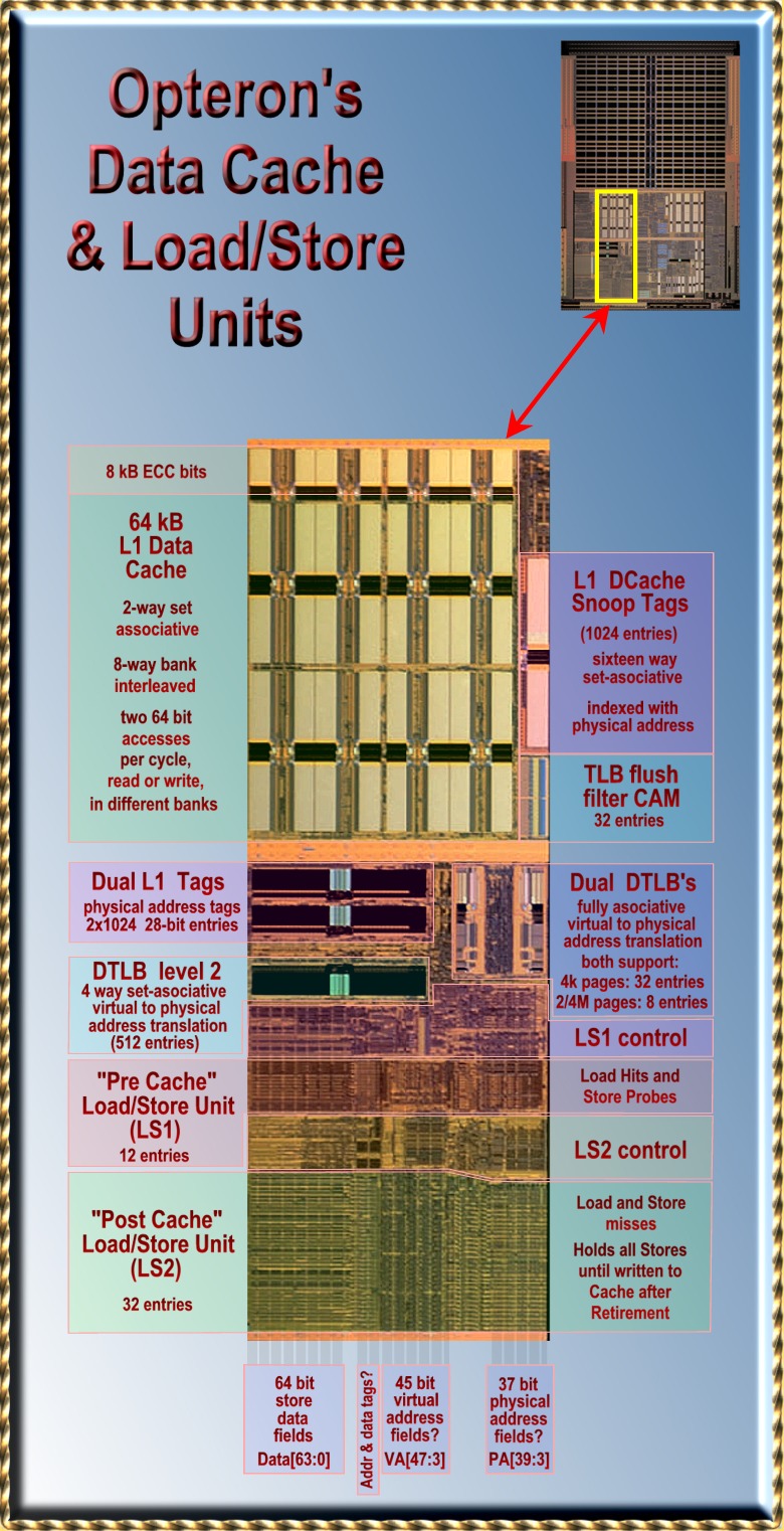
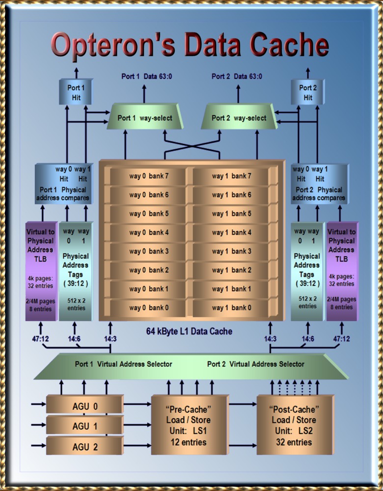
3.1
Data Cache: 64 kByte with three cycle data
load latency
|
|
The
Opteron's relatively large L1 Data Cache
supports a three cycle Load-Use
latency. Actually only the second
and third cycle are used to access the Cache
memory itself. The first cycle is spend in the
Integer Pipeline for the x86 memory address
calculation using one of the three available
AGU's. The address calculated by the AGU is
send to the memory array in the second cycle
where it is decoded. This
means that it is known at which word line the data
can be found at the end of the second
cycle.
The right
data word is activated at the beginning of the
third cycle. Data is accessed in the memory
array, selected and send forward to the
Integer Pipeline or the Floating Point
pipeline. Below the more detailed timing of a
typical Integer x86 instruction
F(
reg,mem ). This type of
instruction first loads data from memory and
then performs an operation on it.
We
see that in the same cycle in which the
instruction is dispatched to the Scheduler it
is also dispatched to the so-called "Pre-Cache
Load/Store unit" or simply
LS1. Instructions
in this unit compete for cache access together
with those in LS2. The instructions in
LS1 first need to wait for their effective
memory address. They monitor the result busses
of the AGU's. An instruction in LS1 knows from
which AGU it can expect its address.
Instructions check the re-order buffer Tag
which identifies the address one clock-cycle
in advance. In general, an instruction in LS1
will fetch its address and wait for its turn
to probe the cache.
|
Typical timing
of an F ( reg, mem ) x86
operation.
|
Cycle
|
Integer
Scheduler
|
Load / Store
Unit
(LS1)
|
ALU's
and
AGU's
|
Cache
Address
Decode
|
Cache
Data
Access
|
|
0
|
Dispatched
to
Scheduler
|
Dispatched
to
LS1
|
|
|
|
|
1
|
AGU
Scheduled
|
|
|
|
|
|
2
|
|
Load
Scheduled
|
Address
Generation
|
|
|
|
3
|
|
|
|
Cache
Address
Decode
|
|
|
4
|
ALU
Scheduled
|
|
|
|
Cache
Data
Access
|
|
5
|
|
|
Dependent
Operation
|
|
|
|
Instructions
may route the address immediately to the cache
also if there are no other (older)
instructions waiting. This is the case in our
example above. In any case, each instruction
will keep the address for possible follow-on
actions. The address is send directly from the
AGU result bus to the Data Cache's address
decoders in our case here. Data comes
back from memory one cycle later and is routed
to the Integer Pipeline. LS1 places the
re-order buffer Tag one cycle in advance on
the Data Cache result Tag bus so that the
Integer ALU schedulers can schedule any
instruction depending on the load
data.
|
|
3.2 Two
accesses per cycle, read or
write: 8 way bank interleaved,
two way set associative
|
|
The
Opteron's cache has two 64 bit ports. Two
accesses can occur each cycle. Any combination
of loads and stores is possible. The dual port
mechanism is implemented by a banking
mechanism: The cache consist of 8 individual
banks, each with a single port. Two accesses
can occur simultaneously if they are to
different banks.
|
Virtual Address
bit used to access the L1 data
Cache
|
Cache
Line Index
|
Bank
|
Byte
|
|
14
|
13
|
12
|
11
|
10
|
9
|
8
|
7
|
6
|
5
|
4
|
3
|
2
|
1
|
0
|
|
A single
64 byte cache line is subdivided in 8
independent 64 bit banks. Two accesses are to
two different banks if their addresses have a
different bank-field, address bits 3 to
5. The bits are the lowest possible
address bits that can be used for this
purpose. This schem effectively maps adjacent
64 bit words in different banks. The principle
of data locality makes
these bits the most suitable choice.
The 64
kByte Cache is two way set-associative. The
cache is split in two 32 kByte ways accessed
with Virtual Address bits [14:0]
A hit into
any of the two ways is detected if the Physical
Address Tag, bits [39:12], which is
stored alongside with each cache line, is
identical to bits [39:12] of the Physical
Address. Virtual to
Physical address translation is performed with
the help of the TLB's (Translation Look
aside Buffers). A port accesses 2 ways
and compares 2 tags with the translated
address. Each port has its own TLB to do the
address translation.
The two 64
bit ports are used simultaneously when
exchanging cache-lines with the rest of the
memory hierarchy. This means that the memory
bus from the unified L2 cache to the L1 data
cache is now 128 bit wide. The event where a
new cache line is needed will take first 4
cycles to evict the old cache-line and then 4
cycles more to load the new cache-line when it
arrives.
|
|
|
|
|
|
|
|
|
|
3.3 The Data
Cache Hit / Miss Detection: The cache
tags and the primairy TLB's
US Patent 6,453,387.
|
|
The
L1 Data Cache has room to store 1024 cache
lines out of the total of 17,179,869,184 cache
lines that fit within the 40 bit physical
address space. Accesses need to check if
the stored cache line corresponds with the
actual memory location they want to access. It
is for this purpose that the Tag rams store
the higher physical address bits belonging to
each of the 1024 cache-lines. There are two
copies of the Tag ram to allow the
simultaneous operation of two access
ports.
The Tag
rams are accessed with bits [14:6] of the
virtual address. Each Tag ram outputs 2 Tags
for both ways of the 2
way- set-associative cache. The wanted
cache-line can be in either way. The Tag rams
contain physical addresses. A physical address
uniquely defines a memory position throughout
the entire distributed system memory.
The cache
is however accessed with the virtual addresses
as defined by the program. Virtual addresses
have only a meaning from within a process
context. This means that a virtual-to-physical-address
translation is needed to be able to
check the physical Tags. This translation is
handled by a lengthy sequence of four table
lookups in memory: The virtual address
field [47:12] is divided into four equal
sub-fields that each indexes into one of the
four tables. Each table points to
the start of the next table, The last table,
the page table, then finally contains the
translated address.
|
Virtual Address
to Physical Address
Translation: The Table
Walk.
|
virtual
address
|
page
offset
|
|
page
map level 4
table
offset
|
page
directory
pointer
offset
|
page
directory
offset
|
page
table
offset
|
|
47
39
|
38
30
|
29
21
|
20
12
|
11
0
|
|
|
|
|
|
|
|
|
|
|
|
|
|
|
|
|
|
|
|
|
|
|
==>
|
|
|
|
|
|
|
|
|
==>
|
|
|
|
|
|
|
|
==>
|
|
|
|
|
|
|
|
|
|
|
|
|
physical
address
|
page
offset
|
|
39
12
|
11
0
|
|
|
This
so-called Table-Walk is a very lengthy
procedure indeed. The Opteron uses so-called
Translation Look aside Buffers (TLB's) to
remember the 40 most recently used address
translations. 32 of these remember 4k page
translations using the scheme above. The
remaining 8 are used for so-called 2M / 4M page
translations which skip the last table and
define the translations for large 2 Megabyte
pages. ( The 4M pages are only used for
backwards compatibility )
The virtual
address bits {47:12] are compared with all 40
entries of the TLB's in the second of the
three clock-cycle access. At the end of the
second cycle we know if any one of them
matches. Each entry also contains the
associated physical address bits
[39:12]. These are selected in the third
cycle and compared with the physical Tags to
test if we have a cache hit.
|
|
3.4 The 512
entry second level TLB
|
|
If the
necessary translation is not found within the
40 entries of the primary TLB's, then
there is a second chance that it is available
in the level-2 TLB which is shared by
both ports. This table contains 512
address translations. This larger table can be
used to update the primary TLB's with a
minor delay. It is organized in a
different way: It is 512 entry
4-way set-associative.
This means
that it has 128 sets of 4 translations
each. Virtual address bits [18:12] are
used to select one of the 128 sets. We
get four translations giving us four chances
that we have the translation we need.
Each translation contains the rest of the
virtual address bits [47:19]. We can
check if we have the right translation by
comparing these bits with our address.
The matching entry then contains the
associated physical address field [39:12] we
need.
|
|
3.5 Error
Coding and Correction
|
|
The L1
Data Cache is ECC protected (Error Coding and
Correction). Eight bits are used
for each 64 bits to be able to correct single
bit errors and to detect dual bit errors with
the help of a 64 bit Hamming SED/DED scheme
(Single Error Detection / Double Error
Detection) Six parity bits are needed to
retrieve the position of the error bit.
|
|
E
C
C
|
64 bit
Hamming SED/DED error
location
retrieval
|
|
bit
63
bit 0
|
|
|
0
|
1
|
1
|
0
|
1
|
0
|
1
|
0
|
1
|
1
|
1
|
0
|
1
|
1
|
0
|
0
|
1
|
1
|
1
|
1
|
0
|
1
|
x
|
0
|
1
|
0
|
1
|
0
|
1
|
1
|
1
|
0
|
0
|
0
|
1
|
0
|
1
|
1
|
0
|
0
|
0
|
1
|
0
|
1
|
1
|
0
|
1
|
1
|
0
|
1
|
0
|
1
|
0
|
1
|
1
|
0
|
1
|
0
|
1
|
0
|
1
|
1
|
1
|
0
|
|
0
|
|
|
|
|
|
|
|
|
|
|
|
|
|
|
|
|
|
|
|
|
|
|
x
|
|
|
|
|
|
|
|
|
|
|
|
|
|
|
|
|
|
|
|
|
|
|
|
|
|
|
|
|
|
|
|
|
|
|
|
|
|
|
|
|
|
|
1
|
|
|
|
|
|
|
|
|
|
|
|
|
|
|
|
|
|
|
|
|
|
|
x
|
|
|
|
|
|
|
|
|
|
|
|
|
|
|
|
|
|
|
|
|
|
|
|
|
|
|
|
|
|
|
|
|
|
|
|
|
|
|
|
|
|
|
1
|
|
|
|
|
|
|
|
|
|
|
|
|
|
|
|
|
|
|
|
|
|
|
x
|
|
|
|
|
|
|
|
|
|
|
|
|
|
|
|
|
|
|
|
|
|
|
|
|
|
|
|
|
|
|
|
|
|
|
|
|
|
|
|
|
|
|
0
|
|
|
|
|
|
|
|
|
|
|
|
|
|
|
|
|
|
|
|
|
|
|
x
|
|
|
|
|
|
|
|
|
|
|
|
|
|
|
|
|
|
|
|
|
|
|
|
|
|
|
|
|
|
|
|
|
|
|
|
|
|
|
|
|
|
|
1
|
|
|
|
|
|
|
|
|
|
|
|
|
|
|
|
|
|
|
|
|
|
|
x
|
|
|
|
|
|
|
|
|
|
|
|
|
|
|
|
|
|
|
|
|
|
|
|
|
|
|
|
|
|
|
|
|
|
|
|
|
|
|
|
|
|
|
0
|
|
|
|
|
|
|
|
|
|
|
|
|
|
|
|
|
|
|
|
|
|
|
x
|
|
|
|
|
|
|
|
|
|
|
|
|
|
|
|
|
|
|
|
|
|
|
|
|
|
|
|
|
|
|
|
|
|
|
|
|
|
|
|
|
|
|
The six
bits are shown in the column at the left. A
one means that a parity error was detected.
The six bits represent the parity of the 32
purple bits in each rows. The parity errors
together now represent a 6 bit index that
points to the error position. Additional
parity bits are used to detect double bit
errors and errors in the parity bits
themselves. (Thanks to Collin for bringing
this to my attention)
|
|
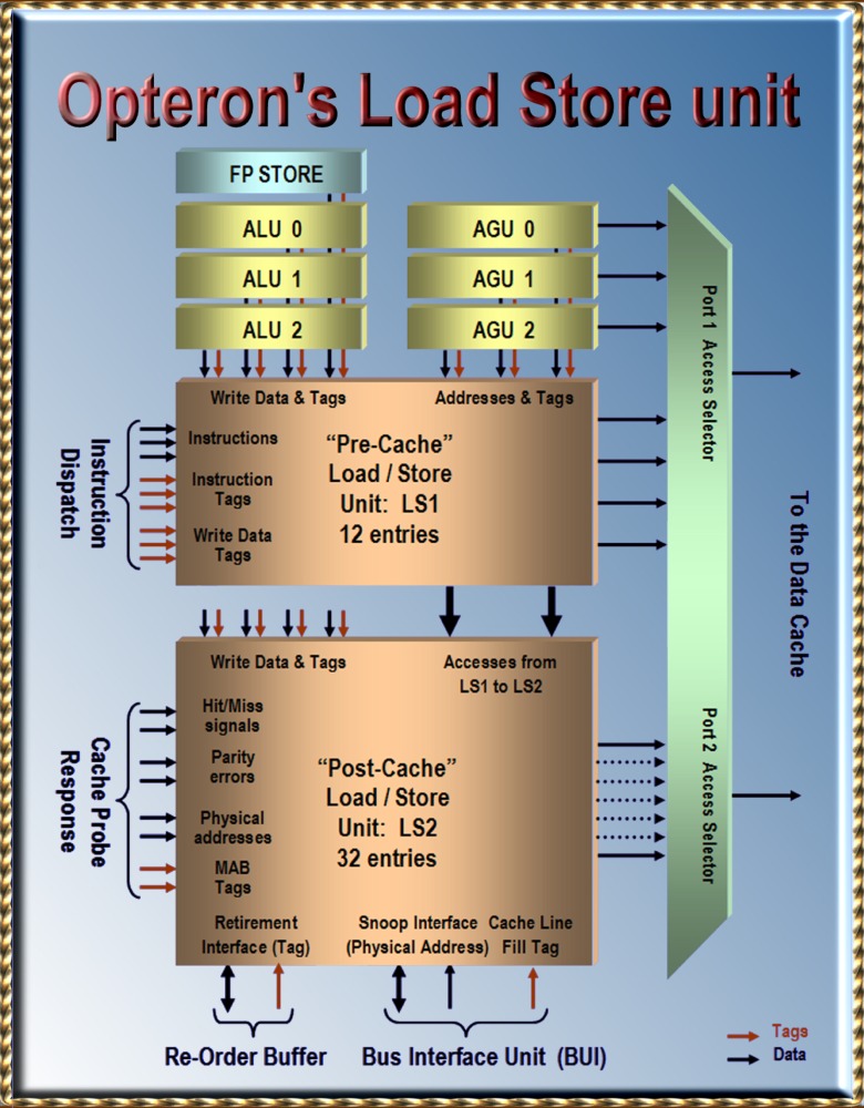
3.6 The
Load / Store Unit, LS1 and LS2
|
|
The Load
Store unit handle the accesses to the Data
Cache. This type of unit plays an increasingly
important role play in modern speculative
out-of-order processors. They are expected to
grow significantly in size and complexity in
newer architectures on the horizon. An
extra reason to give the Opteron's Load Store
units a closer look. The split in LS1 and LS2
is sometimes described as LS1 being for the L1
Data Cache and LS2 for the L2 Cache. This is
far to popular however and even incorrect.
We'll go into more detail here.
|
|
|
|
|
|
|
|
|
|
3.7 The "Pre
Cache" Load / Store unit: LS1
|
|
The
Pre-Cache Load/Store unit (LS1) is the place
where dispatched memory accesses wait for the
addresses generated by the AGU's (Address
Generator Units) LS1 has 12
entries, whenever a memory access is
dispatched to the Integer Scheduler it is also
dispatched to an entry in LS1. The re-order
tag bus belonging to the AGU indicates if the
required Address is being calculated and
available on the result bus of the AGU in the
next cycle. An access waiting in LS1 knows at
which AGU to look for the address.
When an
instruction has its address coming or did
already receive it may then probe the cache.
There are two access ports. The two oldest
accesses in LS1 will be allowed to probe the
Cache. Both load and store instructions probe
the cache. A load will actually access the
cache to obtain the load data. The store
presents its address but will never write from
LS1 to the Cache. Store instructions will only
write after they've received the data to be
written and when they are retired.
Stores
must be retired first because the store
instruction may be speculative and is
discarded later. Imagine that MicroSoft
patches a buffer overflow exploit by adding a
test for the overflow. This test becomes a
conditional branch that prevents the write to
the buffer in case of an overflow. The
overflow tends to never happen so the branch
predictor will predict it as not-taken, It
will do so also in the case that it finally
does happen. The write to the buffer will now
be executed speculative.
So the
actual writes to the cache must be delayed
until after retirement when it's verified that
the branch predictions were correct.
These
deferred stores do not introduce any real
delays however. Loads that access the cache
also check LS1 and LS2 to see if there are any
pending writes to the memory location they are
about to read. If so than they catch the data
directly from LS1 or LS2 without delay.
The stores
in LS1 however do present their address to the
cache hit/miss detection logic. If it turns
out that the cache-line is not present then it
may be loaded as soon as possible from the
Level 2 cache or from system memory.
This can be a good policy since there is a
significant chance that following loads will
need the same cache-line. Stores may receive
the data they have to write to memory while
waiting in LS1 as long as the data comes in
time, otherwise they move on to LS2 to receive
the data there.
|
|
3.8 Entering
LS2: The Cache Probe Response
|
|
All
accesses in LS1 probe the Cache and then move
on to the Post-Cache Load/Store unit ( LS2 )
An access
can either be a Load, a Store or a
Load-Store (The latter reads first and
then writes the result back to the same
location)
All
accesses which came from LS1 first wait to see
the results from the cache probe. If it was a
cache hit or a miss, If there was a cache
parity error. They also receive the physical
address which was translated from virtual into
physical by the TLB's. Together with the
physical address come the page attribute bits
which determine for instance if the memory is
cacheable or not.
Then in
the following cycle, in case there was a cache
miss, the instructions receive a so-called
MAB
tag (
Missed Address Buffer Tag ) This tag
will later be used to see if a missed
cache-line arrives from the L2 cache or from
system memory. The MAB tag needs to be
used instead of the generally used re-order
buffer tags. Multiple Loads and Stores may
depend on the same cache line and thus on the
same MAB tag. All these accesses miss
and they'll all receive the same MAB
tag.
The Bus
Interface Unit (BUI) will load missed
cache-lines from the unified L2 cache or
system memory to fill the data-cache. It also
presents the so-called Fill-tag to LS2.
This fill-tag is compared to the MAB-tag of
all accesses that missed. The accesses that
match the fill-tag are changed from miss to
hit.
|
|
3.9 The "Post
Cache" Load Store unit: LS2
|
|
The
so-called Post-Cache Load Store unit ( LS2 )
has 32 entries. It is organized in a somewhat
"shift register" like way so that the oldest
outstanding access ends up in entry
0. Each of the 32 entries has
numerous fields. Many of these fields are
accompanied with a comparator and other logic
to see if the fields matches a certain
condition. All accesses stay in LS2 at
least until retirement, Accesses that missed
the cache will wait in LS2 until the
cache-line arrives from the memory
hierarchy. All Stores wait in LS2 for
their retirement first before actually writing
data to memory.
|
Various fields
in an LS2 buffer entry
|
|
|
Type
|
Address
& Data
|
Tags
|
Status
Flags
|
Action
Flags
|
....
|
|
|
|
|
|
|
|
|
Valid
Flags
|
Acc.
Type
|
Store
Data
64
bit
|
Virtual
Address
|
Physical
Address
|
mem
Type
|
Instr-
uction
Tag
|
Write
Data
Tag
|
Missed
Address
Buffer
Tag
|
Cache
Hit
/
Miss
|
Retired
access
|
Last
Store
in
Buff
(LIB)
|
Self
Mod.
Code
Flag
|
Snoop
Re-
Sync
Flag
|
Store
Load
For-
ward
|
....
|
|
|
|
Retired
Stores in LS2 that have the hit/miss flag set
to hit may use a cache port simultaneously with a
probing store in LS1. The retired store from
LS2 writes to the data cache itself but does
not use the cache hit/miss logic. The probing
store from LS1 only uses the hit/miss logic
but doesn't access the data cache itself. This
shared use is important performance wise
because each store would occupy a cache port
twice otherwise, first while probing from LS1
and secondly when writing from LS2 after
retirement. This would halve the store
bandwidth of the L1 Data Cache.
|
|
3.10 Retiring
instructions in the Load Store unit and
Exception Handling
|
|
All access
instructions, Loads as well as Stores stay in
LS2 until they are retired. Loads may be
removed directly from LS2 when they are
retired to make place for new instructions.
Stores must still write their data to memory.
They wait to do so until retirement when it is
determined that no exception or branch
miss-prediction occurred. Writes are
removed from LS2 after they have committed
their data to memory.
LS2 has a
retirement interface with the re-order
buffer. The re-order buffer presents the
Tag of the line that is being retired to LS2.
It only
needs to present a single Tag for up to three
instructions in a line since these all have
the same tag except for the 'sub- index' which
identifies the lane (0, 1 or 2).
LS2 compares all-instruction tags with the
retirement-tag and set the Retired
flag of those who match. Retired loads may
be deleted directly from LS2.
If the
retirement logic of the re-order buffer has
detected a branch-miss prediction or exception
then all instructions matching the retirement
tag and all those with succeeding tags are
discarded from LS2. The only ones left in LS2
are the retired stores that are waiting to
commit their data to memory.
|
|
3.11 Store to
Load forwarding, The Dependency Link
File
US Patent 6,266,744.
|
|
A Load
probing the data cache will also check the
Load Store units to see if there are any
outstanding stores to the same address as the
load. If it finds such a store ( and the store
is before the load in program order ) then
there are two possibilities. If the store has
already obtained the write data from one of
the result busses then these can be directly
forwarded to the load. If the store has not
yet obtained it data then the load misses and
moves to LS2.
An entry
is created in a unit called the
Dependency Link File. This
unit now registers both the tags of the write
data, ( which tells the data-to-be-stored is
coming in the next cycle ) as well as the Load
tag which is the be used to tell a following
instruction that the load data will be
available. The Dependency Link File keeps
monitoring the write data tag, and then, as
soon as it detects it, puts the load
instruction tag on one of the Cache Load tag
busses.
It does
the same with the actual data when it comes
one cycle later. The result data from
instruction 1 can be directly forwarded to the
consuming instruction 4 in the example below.
Instructions 2 and 3 (the store and the load)
are bypassed in this case.
|
1) F(
regA,regD
);
//
register A is a function of
register A and register D
2)
store ( mem, regA ); // store register
A to memory
3)
load ( regB, mem ); // load register B
from the same memory location
4) F(
regD, regB
); // uses register B
and register D to calculate new
value of register D
|
Miss-matched
store to loads: Stores that only modify part
of the load data are not supported. The load
must first wait unit the store is retired and
stored to memory. The load may then access the
cache to get it's data which is a combination
of the stored data and the original contents
of the cache. The optimization manual
describes all possible miss-match cases since
they can lead to a considerable performance
penalty.
Multiple
Stores to the same address are handled with
the so-called LIB flag ( Last In Buffer ) This
flag identifies the most recent store to a
certain address. A newer load accessing the
same address will choose this one. Multiple
partial stores to the same word were each
modifies only a part of the word are not
supported by the Load Store buffer. They are
not merged in the Load Store buffer. They will
be merged later on in the cache after all
stores are retired and written.
|
|
3.12 Self
Modifying Code checks: Mutual
exclusive L1 DCache and L1 ICache
US Patent 6,415,360.
|
|
Self
Modifying Code (SMC) checks must in principle
be performed for each store. It must be tested
if the store does not modify any of the
instructions in the Instruction Cache or any
following Instruction in flight in any stage
of execution. A significant simplification is
made by making the L1 Data Cache and L1
Instruction Cache exclusive to each
other: A cache-line can only exist in either
one, not in both at the same time. When a
cache line is loaded in the L1 Data cache then
it will be evicted from the L1 Instruction
cache.
The first
advantage is that the contents of the
Instruction Cache does not need to be tested
any further for SMC. The second advantage is
that SMC checks may be limited to Data Cache
misses. Stores to un-cacheable memory must be
checked always.
( They
always "miss" ) The store's write-address is
send from LS2 to the SMC test unit which is
close to the Instruction Cache. This units
holds the cache-line addresses of all the
Instructions in flight. If there is a conflict
then it marks the store that caused the
conflict. The reorder buffer will discard
all instructions which follow the store when
the store is retired.
|
|
3.13 Handling
multi processing deadlocks:
exponential back-off
US Patent 6,427,193.
|
|
Deadlocks
can occur when multiple processors fight for
the ownership of the same cache-line. They do
so for instance if they both want to write to
the same line. A cache-line is generally
loaded as soon as possible in case of a
cache-miss. This will cause the cache-line to
be invalidated in other caches in case of a
store. Two processors get in a deadlock if
they keep invalidating each others cache-lines
before they are able to finish the stores.
An example
given is the case where two processor try to
complete a store which is to an unaligned
address so that part of the store data goes to
cache line A1 and part of the store data goes
to cache line A2. Unaligned stores of this
type are typically split into two stores by
the hardware. An exponential
back-off mechanism is provided to
handle this kind of deadlock situations. A back-off time is
introduced when the memory access remains
unsuccessful before retrying to become owner
of the cache-line again. This time grows exponentially after
each unsuccessful try until one of the
processors finally succeeds.
|
|
3.14
Improvements for multi processing and multi
threading
|
|
|
The Opteron's micro
architecture has a large number of
improvements related to multi
processing and multi threading.
Very important improvements also
for the desktop market.
Multi-processor on a chip
solutions are just around the
corner and hyper- threading may
take a significant step forward in
the near future with Intel's
Prescott.
The ability to perform
multi processing and multi
threaded applications efficiently
becomes essential. Switching
contexts, starting and ending of
processes and threads as well as
inter-process and inter-thread
communication is traditionally
associated with large overheads.
Significant improvements have been
made to reduce these overheads to
a minimum.
|
|
|
|
|
3.15 Address
Space Number (ASN) and Global
flag
US Patent 6,604,187.
|
|
Different
processes can have different contexts That is:
different translations from virtual to
physical addresses. A process switch will
cause the Translation Look Aside buffers to be
invalidated ( flushed ). Large Translation
buffers won't help you a lot if they are
frequently flushed which then can lead to
significant performance degradation. The
Opteron introduces a new mechanism to avoid
flushing of the TLB's. An Address
Space Number (ASN) register is added
together with an enable bit (ASNE).
The Address
Space Number is used to
uniquely identify a process. Each entry
in the TLB now includes the ASN of the
process. An address can be successfully
translated if the address matches the Virtual
Address Tag in the TLB and
the
ASN register matches the ASN field in the TLB.
The ASN field can be seen as an "extension" of
the Virtual Address. This now means that
different translations of different processes
can coexist in the TLB, avoiding the need to
flush the TLB's for context switches.
A global
flag is available for data and code that
is preferably accessible for all processes,
typically operating system related. Global
translations do not require the ASN fields to
match. This means that many processes can
share a single entry in the TLB to access
global data. Another advantage of the
ASN and global flag is that flushing can be
limited to specific entries whenever an
invalidation of the TLB is needed. Only
the entries which have a certain ASN or have
the global bit set are flushed.
|
|
3.16
The TLB Flush Filter
CAM
US Patent 6,510,508.
|
|
The TLB's
can be seen as caches containing the
translation information stored in the address
translation tables in memory. The actual
translation requires several levels of
indirections through the tables stored in main
memory. This is the so-called "table walk"
A very
time consuming process which may take many
hundreds of cycles for a single TLB entry. The
Opteron attempts to speed up the table walk
with a 24 entry Page Descriptor Cache.
Even so,
it remains important to avoid the table walk
whenever possible in a multi-tasking
multi-threaded environment. A table walk
becomes necessary whenever entries in the TLB
do not correspond to the memory resident
translations anymore because some- body has
modified the
latter.
Until now
there was only one way to guarantee TLB
coherency: Flush the TLB's if it may be
possible that any of the entries is not
identical anymore to the memory resident
tables. Many actions in the x86 architecture
result in an automatic flush of the TLB's,
often unnecessary. A new feature in the
Opteron: The TLB flush filter can avoid these
costly flushing in many occasions.
The TLB
Flush filter is implemented as a 32 entry,
Content Addressable Memory ( CAM ). It
remembers the addresses of regions in memory
that were accessed when the TLB's were
loaded. These regions thus belong to the
Page Translation Tables. The Filter then keeps
monitoring all accesses to memory to see if
any of these regions are accessed again. If
not then it may disable the flushing of the
TLB's because coherency is guaranteed.
|
|
3.17
Data Cache Snoop Interface
|
|
The Snoop
interface is used for a wide variety of
purposes. It's used to maintain Cache
Coherency in a multiprocessor system. It is
used for conserving strict memory ordering in
shared memory, for Self Modifying Code
detection, for TLB coherency et-cetera.
The snoop
interface uses the physical addresses from
other processor accesses as well as from
accesses issued on behalf of the instruction
cache to probe various memories and buffers
for data that has somehow, something to do
with that particular address.
|
|
3.18
Snooping the Data Cache for Cache
Coherency, The MOESI protocol
|
|
The
Opteron can maintain cache coherency in
systems of up to 8 processors. It uses the
so-called MOESI protocol
for this purpose. The snoop interface plays a
central role in the effectuation of the
protocol.
If a cache
line is read from system memory ( which may be
connected to any of the eight processors ),
then the read has to snoop all the caches of
all processors. Snoop accesses are much
smaller then normal memory accesses because
they do not carry the 64 byte cache line data.
Many snoops may therefore be active without
overloading the distributed memory system
throughput. A snoop may find the cache-line in
one of the caches of another processor.
If a
processor does not find the cache-line in
someone else's cache then it loads it from
system memory into its cache and marks it as Exclusive. Now
whenever it writes something in the cache-line
then it becomes Modified. It does
in general not write the modified cache-line
back to memory. It only does so if a special
memory-page-attribute tells it to do so (write
through). The cache line will be evicted only
later on if another cache-line comes in which
competes for the same place in the cache.
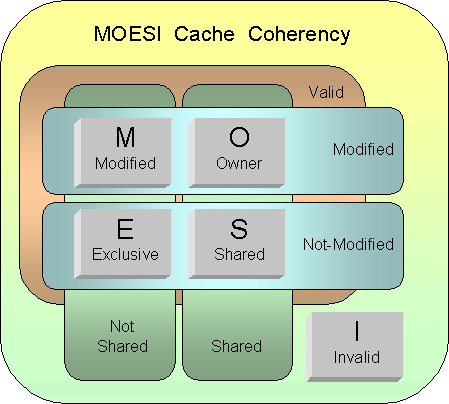
If a
processor needs to read from memory and it
finds the cache line in someone else's cache
then it will mark the cache line as Shared. If the
cache-line it finds in the other processors
cache is Modified then it
will load it directly from there instead of
reading it from the memory which may be not up
to date. Cache to cache transfers are
generally faster then memory accesses.
The status
of the cache-line in the other cache goes from
Modified
to
Owner. This
cache-line still isn't written back to memory.
Any other (third) processor that needs this
cache-line from memory will find a Shared version
and a Owner version
in the caches of the first two processors. It
will obtain the Owner version
instead of reading it from system memory. The
owner is the latest who modified the
cache-line and stays responsible to update the
system memory later on.
A
cache-line stays shared as long as nobody
modifies the cache-line again. If one of the
processors modifies it then it must let this
know to the other processors by sending an
invalidate probe throughout the
system. The state becomes Modified in this
processor and Invalid in the
other ones. If it continues to write to the
cache line then it does not have to send
anymore invalidate probes because the cache
line isn't shared anymore. It has taken over
the responsibility to update the system memory
with the modified cache line whenever it must
evict the cache-line later on.
|
|
3.19
Snooping the Data Cache for Cache
Coherency, The Snoop Tag RAM
|
|
Other
processors that access system memory need to
snoop the Data Cache to maintain cache
coherency using the MOESI protocol. We saw
that there were two kinds of snoops. Read and
Invalidate snoops. The basic task of a snoop
is first to establish if the Data Cache
contains the cache-line in question. There is
a third set of Tags available specially for
the snoop interface. ( The other two are used
for the two regular ports of the data cache ).
The snoop-Tag ram has 1024 entries, one for
each cache line. It holds the Physical
address bits [39:12] belonging to each cache
line.
|
Virtual Address
bit used to access the L1 data
Cache
|
virtual
page address
|
offset
in page
|
offset
in cache line
|
|
W
|
14
|
13
|
12
|
11
|
10
|
9
|
8
|
7
|
6
|
5
|
4
|
3
|
2
|
1
|
0
|
Physical
Address used to snoop the L1
data Cache
|
physical
page address
|
offset
in page
|
offset
in cache line
|
|
15
|
14
|
13
|
12
|
11
|
10
|
9
|
8
|
7
|
6
|
5
|
4
|
3
|
2
|
1
|
0
|
|
The
regular Tag rams are accessed with the virtual
address. The Snoop Tag ram however must deal
with the physical address ! Fortunately many
of the virtual address bits needed are
identical to the physical address bits. Only
bits [15:12] are different and thus useless.
This means that we must read out the Tags of
all 16 possible cache-lines in parallel and
then test if anyone of them matches. Luckily
enough this doesn't present to much of a
burden. The total bus width (in bit-lines) of
for instance the cache rams is 512 bit.
Sixteen times a 28 bit Tag is less (448) so
there's space left for some extra bits like
the state info for each cache-line.
Once we
know which of the 16 possible cache-lines hits
then we know also the remaining virtual
address bits needed to access the cache plus
the Way (0 or 1) which holds the cache-line.
The position itself, ( 1 out of 16 ) directly
provides the 3 extra address bits plus the Way
bit. This means we can now access
the cache if needed in case of a Read Snoop
hit.
|
|
3.20
Snooping the L1 Data Cache and outstanding
stores in LS2
|
|
It is not
necessary for snoop reads from
other processors that want to read a
cache-line from the L1 data cache to check for
retired stores in LS2 that will write to the
cache-line they are about to read. This
even though the data these stores will write
is already considered to be part of the memory
by the processor who issued the writes.
It's is OK for other processors to see these
writes occur at a later stage. The only effect
externally is that it looks as if the
processor is slightly slower.
An
external processor that writes to a shared
cache line must send snoop
invalidates around. The snoop
interface will invalidate the local cache-line
if it receives such a snoop invalidate that
hits the cache. The snoop interface must also
set the hit/miss flag to miss for all
stores in the Load Store unit that want to
write to the cache-line that was
hit. The later is not a specific
snoop operation however. It is needed in
all cases in which a cache-line is evicted or
invalidated. These stores that originally did
hit but who are set back to miss will need to
probe the cache again.
|
|
3.21
Snooping LS2 for loads to recover strict
memory ordering in shared memory US Patent 6,473,837.
|
|
An
interesting trick allows the Opterons to
handle speculative out of order loads from
shared memory and still observe the strict
memory access ordering required for shared
memory multiprocessing. The hardware detects
violations and can restore strict memory
ordering when needed. A
communicating processor may for instance first
write a new command for another processor to
A1 in memory and then increment a value A2 to
notify that it has issued the next
command. The processor which is supposed
to handle the commands may find the value A2
incremented but still reads the old command
from A1 if it executes loads out of order.
The
ability to handle loads out of
order can significantly speed up
processing. Most notable is the example where
a first load misses the cache. An out of order
processor may issue another load which may hit
the cache without waiting for the result of
the first load. It would be beneficial
to maintain out-of-order loads in a
multiprocessing environment.
Another
important speed improvement is speculative
processing. The first load that
missed may have been the counter A2 in our
example. The new command must be fetched if A2
has been increased. A conditional call is made
based on a test of the value of A2. A
speculative processor attempts to predict the
outcome of the branch at the beginning of the
pipeline. It may predict that the counter has
been incremented if it generally takes more
time to execute the command than it takes to
provide a new command.
That is:
The new command is generally sitting waiting
to be executed by the time the previous
command has been executed.
The
speculative out of order processor may first
attempt to load the counter A2, It may miss
but the branch predictor has predicted that it
was increased and the command from A1 will be
loaded for execution. The load from A1 may hit
the cache. We actually do not know if this is
a new commando or not. Let say it is the old
one. The counter A2 still has to be loaded
from memory. If A2 is increased in the mean
time then the load that missed will cause the
modified cache-line to be loaded in the local
data cache with the incremented counter
included. The processor will conclude that the
branch prediction was correct and erroneously
carry on with the old command.
The
Opteron has a snoop mechanism that allows this
kind of fully speculative out-of-order
processing for high performance
multi-processing. The mechanism detects cases
which may go wrong and consequently restores
memory ordering. We'll illustrate the
mechanism with the use of our example.
When
the first processor writes a new commando into
A1 then it will send a snoop-
invalidate around to invalidate the
cache-line in all other caches. This snoop
invalidate will also reach the snoop interface
of the Load Store unit:
The snoop
interface first checks the entries for a load
that did hit the cache-line-to-be-invalidated.
This load would then be the "old command" from
A1 in our example. When it finds a load
hit then it continues by checking all older
loads to see any of them is marked as a
miss. This would then be the load of the
A2 counter value in our example. It
marks the Snoop ReSync flag of all
the load misses it finds. This flag will
cause any succeeding instructions to be
canceled when the load is retired including
the instruction that loads A1. The load
of A1 will be re-executed and will now
correctly read the new command from memory.
|
|
3.22
Snooping the TLB Flush Filter CAM
|
|
Snooping
is used to preserve memory coherency. The
function of the TLB flush filter is to prevent
unnecessary flushes of the TLB's. It
does so by monitoring up to 32 areas in memory
that are known to contain page table
translation information which is cached in the
TLB's. These entries must be snooped
also by snoop invalidates from other
processors that may write to the page tables
of our processor. If any of the snoops
hits a TLB flush filter entry then we know
that a TLB may have invalid entries and that
the TLB flush filter may not prevent the
flushing of the TLB's anymore.
The
snoop-invalidates are not send if a processor
is sure that a cache-line is not shared with
other processors . This suggests that the
TLB's (being caches in their own right)
participate in the MOESI protocol for cache
coherency via the TLB flush filter.
The
memory page translation tables ( PML4, PDP,
PDE and PTE entries) may be in cacheable
memory. A special flag has to be set in
the Opteron if the Operating System decides to
put the tables in un-cacheable memory.
(
TLBCACHEDIS in HWCR )
|
|
Chapter 4, Opteron's Instruction Cache and
Decoding
|
|
|
|
|
|
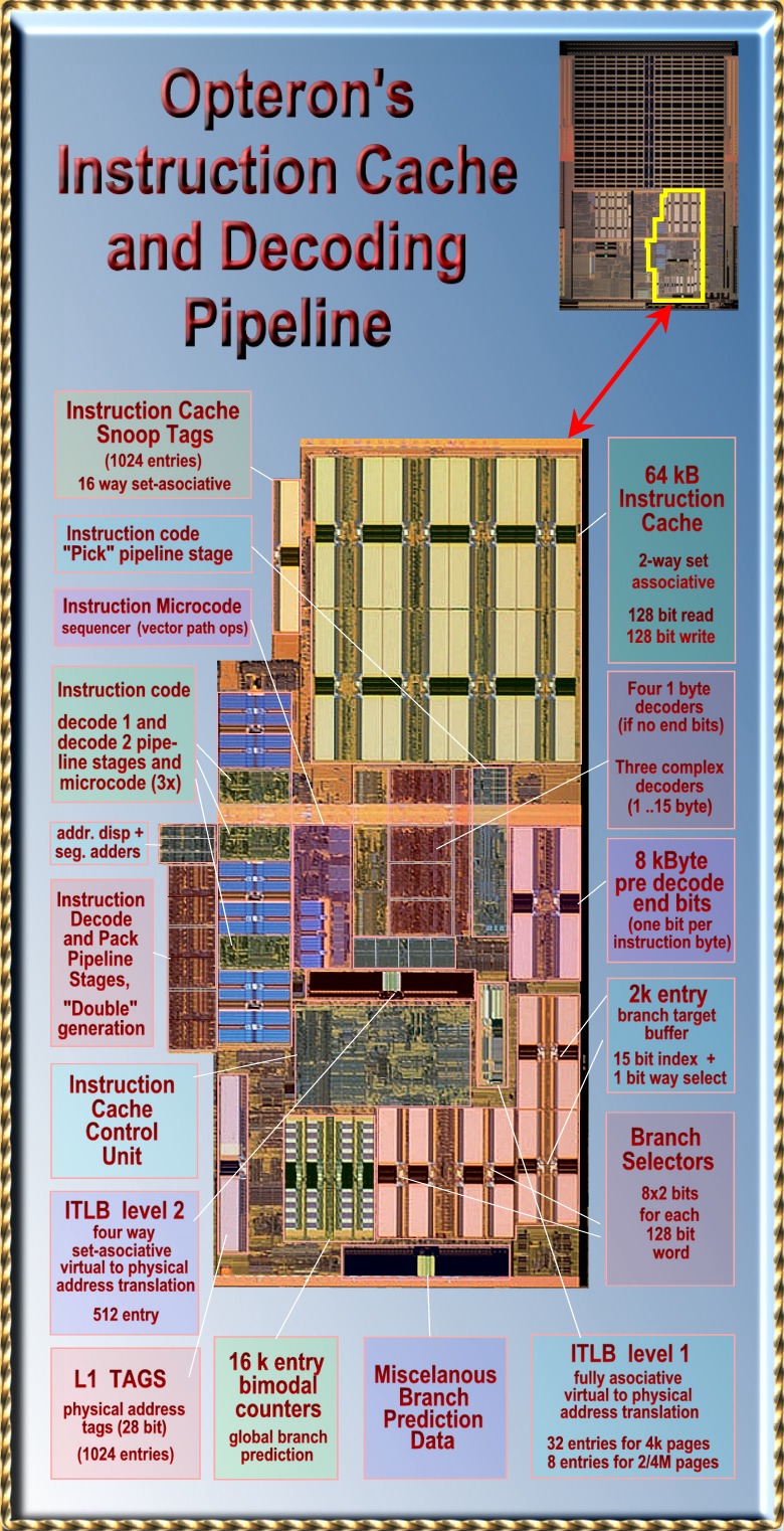
4.1
Instruction Cache: More then
instructions alone
|
|
|
Access to the Instruction
cache is 128 bit wide. 16 bytes of
instructions can be loaded from
the cache each cycle. The
instruction bytes are accompanied
with an extra 76 bits of extra
information. This extends the
total width of the Instruc-
ion cache port to 204 bits.
We're still counting only
the bits that cover the full
Instruction Cache. That is: Each
of the 1024 cache lines has its
own set of these extra bits. There
are several more fields that have
less then 1024 entries and are
valid only for a subset of the
cache lines.
|
|
|
|
Instruction only
|
Total size
|
|
Instruction Cache
size:
|
64 kByte
|
102 kByte
|
|
Cache Line size
|
64 Byte
|
102 Byte
|
|
One Read Port
|
128 bit
|
204 bit
|
|
One Write Port
|
128 bit
|
204 bit
|
|
Well known
are the three so-called pre-decode
bits
attached to each byte. They mark the start and
end points of the complex variable length x86
instructions and provide some functional
information. The other two fields are the
parity
bits, 1 parity bit for each 16 data bits,
and the so-called branch
selectors. ( eight times 2 bit for
each 16 byte line of instruction code ).
|
|
|
Ram Size
|
Bus Size
|
Comments
|
|
Instruction Code:
|
64 kByte
|
128 bit
|
16 bytes instruction
code
|
|
Parity bits
|
4 kByte
|
8 bit
|
One parity bit for each
16 bit
|
|
Pre-decode
|
26 kByte
|
52 bit
|
3 bits per byte (start,
end, function) + 4 bit
per 16 byte line
|
|
Branch Selectors
|
8 kByte
|
16 bit
|
2 bits for each 2 bytes
of instruction code
|
|
TOTAL
|
102 kByte
|
204 bit
|
|
|
The
Opteron's branch selectors are different from
those of the Athlon (32) and they now cover
all 1024 cache-lines of the Instruction
Cache. The branch selectors contain local
branch prediction information which can not
be retrieved as readily as for instance the
pre-decode information. A piece of code has to
be executed multiple times before the
branch-selectors become meaningful.
This is
the reason that the branch selector bits are
saved together with the instruction data in
the unified level 2 cache whenever a
cache-line is evicted from the instruction
cache. The branch selectors represent one bit
extra for each byte. The level 2 cache has
this bit already for ECC ( Error Coding and
Correction ) information. ECC is only used for
data cache lines and not for instruction cache
lines. The latter do not need ECC, a few
parity bits per cache line is
sufficient. Instruction cache lines that
are corrupted can always be retrieved from
external DRAM memory.
|
|
|
|
|
|
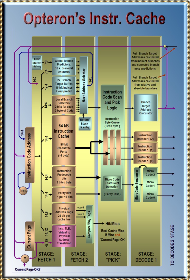
|
|
|
|
4.2 The
General Instruction Format
|
|
A short
overview of the 64 bit instruction format:
A series
of prefixes can precede the actual
instructions. At the start we have the legacy
prefixes. The most important legacy
prefixes are the operand size override prefix
(hex 66) and the address size override prefix
(hex 67). These prefixes can change the length
of the entire instruction because they change
the length of the displacement and immediate
fields which can be 1, 2 or 4 bytes long.
The REX
prefix (hex 4X) is the
new 64 bit prefix which brings us 64 bit
processing. The value of X is used to
extend the number of General Purpose registers
and SSE registers from 8 to 16. Three bits are
used for this purpose because x86 can specify
up to three registers per instruction for data
and address calculations. The fourth bit is
used as operand size override (64 bit or
default size)
|
|
AMD64
Instruction Format
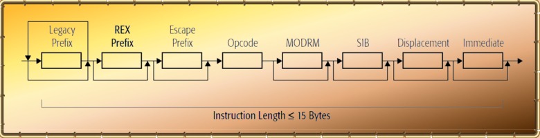
|
|
The Escape
prefix (hex 0F) is used to identify SSE
instructions. The Opcode is the actual start
of the instruction after the prefixes. It can
be either one or two bytes and may have an
optional MODRM byte and SIB byte. The optional
displacement and immediate fields can contain
constants used for address and data
calculations and can be 1, 2 or 4 bytes. The
total length of the instruction is limited to
15 bytes.
|
|
4.3 The
Pre-decode bits
|
|
Each byte
in the instruction cache is accompanied with 3
pre-decode bits generated by the pre-decoder.
These bits accelerate the decoding of the
variable length instructions. Each instruction
byte has a start bit that is
set when the byte is the start of a variable
length instruction and a similar end bit. Both
bits are set in case of a single byte
instruction. More information is given with
the third bit, the function
bit. The decoders look first at the
function bit at the last byte of the variable
length instruction. If the function bit is 0
then the instruction is a so-called direct
path instruction which can be handled
directly by the functional units. Otherwise if
the function bit is 1 at the end byte then the
instruction is a so-called vector
path instruction. A more complex operation
that needs to be handled by a microcode
program.
|
|
Definition
of the Instruction
Pre-decode bits
|
|
START
bit
|
1 indicates first byte
of an instruction
|
|
END
bit
|
1 indicates last byte of
an instruction
|
|
FUNCTION
bit
|
rule
1:
Direct Path
instruction if 0
on the last byte
Vector Path instruction
if 1 on the last
byte
rule
2: 1
indicates Prefix byte of
Direct
Path
(except last byte)
0 indicates Prefix byte
of Vector
Path
(except last byte)
rule
3: For
vector-path instructions
only:
if the function bit of
the MODRM byte is set
then
the instruction contains
a SIB byte.
|
|
Then,
secondly, the function bits identify the
prefix bytes. Ones identify prefix bytes
of direct path instructions and zeroes define
the prefix bytes of vector-path instructions.
Then, finally, in case of vector-path
instructions only: if the function bit of the
MODRM byte is set then the instruction also
contains a SIB byte.
|
|
4.4 Massively
Parallel
Pre-decoding
US Patents 6,460,132 & 6,260,134
|
|
|
We find a very large block
of logic with fourfold symmetry
directly near the position were
the 16 byte blocks of data are
read and written from and to the
instruction cache.
We'll discuss the most
likely candidate here, A fourfold
incarnation of an earlier
pre-decoder described in gate
level detail in US Patent 6,260,134
This fourfold version can,
according to the patent which
describes it, pre- decode an
entire line of 16 bytes in only
two cycles by means of what it
calls: massively parallel
pre-decoding. This circumferences
a basic problem in variable length
pre-decoding and decoding in
general, being:
A second instruction can
not be decoded until the length of
the first instruction is known.
The start position of the second
instruction depends on the length
of the first instruction.
The massively parallel
pre-decoder avoids this problem by
first pre-decoding the 16 possible
instructions in parallel. Each
instruction starts at one of the
16 byte locations of the 16 byte
line. It then filters out the real
instructions with the help of the
program-counter which points to
the start byte of the next
instruction, depending on where we
jump into the 16 byte line.
16 bytes of instructions
can be fetched per cycle from the
instruction cache to be fed to the
decoders. It may be that the line
is not yet pre-decoded or wrongly
pre-decoded. (Data bytes between
instructions can mislead the pre-
decoder).
If a branch is made to an
address which does not have its
pre-decode start bit set then we
know that something is wrong. The
instruction pipeline may invoke
the pre- decoding hardware in this
case to initialize or correct the
pre-decoding bits within only two
cycles.
|
|

|
The
massively parallel pre-decoder uses four
blocks, these blocks are an adapted version of
an earlier pre-decoder. A single block
pre-decodes four possible instructions in
parallel. Each instruction starting at one of
four subsequent byte positions. The old single
block was capable of stepping through a 16
byte line in four cycles. The massively
parallel pre-decoder combines four of them and
uses a second stage to resolve the relations
between the four: The start /
end fixer / sorter.
|
|
4.5 Large
Workload Branch Prediction
|
|
|
Branch Prediction is
the technique that makes it
possible to design pipelined
processors. The outcome of a
conditional branch is generally
only known at the very end of the
pipeline while we need to have
this information at the very
beginning of the pipeline. We need
the branch outcome to know which
line of instructions to load next.
The loading of a line of
instructions already takes two
cycles. If we don't want to loose
anymore cycles then we must have
decided on a new instruction
pointer at the end of the cycle
when 16 instruction byte line
arrives from the instruction
cache.
This means that there is
no time at all to even look at the
instruction bytes, to try to
identify conditional branches, and
then to look up what the behavior
was of these branches in recent
history in order to make a
prediction. Doing this alone would
cost us several cycles.
|
|
|
|
|
4.6 Improved
Branch Prediction
|
|
The Branch
prediction hardware does not make any attempt
to look at the fetched instruction bytes at
all. It uses several data structures instead
to rapidly select a new address. It has
a 2048 entry Branch Target Buffer
and a
12 entry Return Stack to select
a next Program Counter address. It further
uses two branch history structures, one for
local and one for global history, It uses
these branch history structures to predict the
outcome of the branches. The so-called branch
selectors are used for local
history while the global
history counters are used for global
history.
|
|
4.7 The Branch
Selectors |
|
The branch
selectors embody the local history.
Local means that the prediction is based on
the history of the branch itself alone.
Conditional branches that are taken about
always in the same way can be predicted with
the branch selectors. unconditional branches
are also handled by the branch selectors.
Remember that there is no time to look at the
actual code. What a branch selector says is
that history has shown that a branch will be
encountered that is almost certainly taken,
conditional or unconditional.
Now if
it's not so certain that a branch will be
taken? The branch selectors may leave
the prediction in this case to the global
branch prediction. The branch selectors
will predict the branch as taken to identify
the branch but leave the final decision to the
global
history counters by setting the global
flag.
|
| 16
byte line of instruction
code |
|
0
|
1
|
2
|
3
|
4
|
5
|
6
|
7
|
8
|
9
|
10
|
11
|
12
|
13
|
14
|
15
|
|
BS0
|
BS1
|
BS2
|
BS3
|
BS4
|
BS5
|
BS6
|
BS7
|
|
Branch
Selection
|
K7
Athlon 32 |
K8
Athlon 64
|
|
3
|
take branch 2 |
take branch
3 (or
return)
|
|
2
|
take branch 1 |
take branch
2 (or
return)
|
|
1
|
return |
take branch
1 (or
return)
|
|
0
|
continue to next line |
continue to next line
|
|
Each 16
byte line of instruction code is accompanied
with eight 2 bit branch-selectors (some
patents talk about 9) The branch selector
within the line is selected with bits [3:1] of
the Instruction Fetch address. The branch
selector answers the question: I did enter
this 16 byte line on this particular address,
now what 16 byte line should I load in the
next cycle? A line can
have multiple jumps, calls, returns. They can
be conditional or unconditional. We may have
jumped anywhere in the middle of all these
branches. The branch selectors tell us what to
do depending on where we entered the line.
The K7 can
predict two branches per line plus one return.
The new 64 bit core can predict up to three
branches per line and anyone of them may be a
return according to Opteron's optimization
manual. ( There are no patents yet so
the table above is our own extrapolation ).
The branch selectors are saved together with
the instruction code in the large One Megabyte
L2 cache whenever a cache-line is evicted from
the instruction cache. The most useful data to
save there is the information which can't be
easily retrieved from the instruction code:
the branch history. Information like the
actual branch target address or the
fact that the branch is a return is
retrieved relatively fast in most cases by the
processor.
|
|
4.8 The Branch
Target Buffer
|
|
The BTB (
Branch Target Buffer ) contains 2048 addresses
from which the branch selectors can choose the
next cycle's Instruction Fetch address.
Fred Weber's MPF2001 Hammer presentation shows
us that each 16 byte line can now have up to
four branch target addresses to choose from (
Up from two in the case of the Athlon 32
). Each branch target entry is shared
between eight lines. From the branch selectors
we know that any single line may not use more
then 3 of these. We assume that when a branch
selector says: Select the 2nd branch, This
means the second branch available for the
current line.
|
|
Most
important
Branch Target
Buffer fields
|
|
Line
Tag
( 3
bit )
|
15
bit
cache
index
|
Cache
Way
Select,
0 or 1
|
Return
Instruction
|
Use
Global
Prediction
|
Offset
in
Instr.
Code
|
|
Field
|
Description
|
|
Line
Tag ( 3
bit )
|
A branch target buffer
entry is shared between
8 lines.
The line tag tells us if
this entry belongs to
the current
line.
|
|
15
bit cache
index
|
These 15 bits are
sufficient to access the
two 32 kB ways
of the 64 kB 2 way
set-associative
Instruction Cache
|
|
cache
way select
( 0 or 1 )
|
Used to check the way of
the cache..
|
|
Return
Instruction
|
This bit tells us to use
the address from the
return stack
instead to access the
next line in the
instruction cache.
|
|
Use
Global Prediction
|
The Global Flag leaves
the final Branch
Prediction
to the Global History
Counters.
|
|
Offset
in Instruction
code
|
This tells us where the
end of the branch is
located in the
16
byte line of instruction
code.
|
|
Each
branch target entry needs a 3 bit tag to
identify to which of the 8 possible lines of
instructions it belongs. Sharing branch target
entries strongly reduces the amount of branch
target addresses needed. 2048 entries
still would represent 12 kByte if the full 48
bit addresses were stored in the BTB. This
would be a relatively large memory which you
won't find on Opteron's die. The trick used
here is to store only the 16 bits which are
actually needed to access the 64 kByte
instruction cache. The higher address bits are
retrieved later on. The Opteron has a new unit
called the BTAC ( Branch Target Address
Calculator ) to support this.
|
|
4.9 The
Global History Bimodal Counters
|
|
The
Athlon 64 has 16,384 branch history counters.
Four times as much as its 32 bit predecessor.
The counters describe the likelihood that a
branch is taken. They count up to a maximum of
3 when branches are taken and count down to a
minimum of 0 when not taken. Counter
values 3 and 2 predict a branch as taken, see
the table.
|
|
Definition
of the 2 bit Branch
History Counters
|
|
Counter
Value
|
Branch
Prediction
|
|
counter
= 3
|
Strongly Taken
|
|
counter
= 2
|
Weakly Taken
|
|
counter
= 1
|
Weakly not Taken
|
|
counter
= 0
|
Strongly not Taken
|
|
The BHBC
is accessed by using four bits of the Program
Counter and the outcome (taken or not taken)
from the last eight branches. This is
basically the same as in the Athlon 32. The
fact that we now have four times as many
counters means that we have four branch
predictors per 16 byte instruction line. This
corresponds with the four branch target
addresses per line. This would be an
improvement over the Athlon 32 were the two
branches per line could interfere which each
others branch predictions.
|
|
Addressing
the Branch
History Counters
|
|
Instruction
Address
bits 7:4
|
|
|
Branch outcome
of the
eight
previous
branches
|
|
|
| | | |
|
| | | | | |
|
|
|
16,384
Branch History Counters
|
|
|
|
|
|
|
|
|
|
|
|
|
|
|
|
|
Branch
prediction 0
|
Branch
prediction 1
|
Branch
prediction 2
|
Branch
prediction 3
|
|
Another improvement is that
only branches whose global bit was set
participate in the global branch prediction.
This prevents branches with a
static behavior from polluting the global
branch history. ( US Patent 6,502,188
describes this in the context of the
Athlon 32 ) The global bit is set
whenever a branch has a variable outcome.
The GHBC table allows the processors
to predict global branch
patterns of up to eight branches.
|
|
4.10 Combined
Local and Global Branch Prediction with
three branches per line
|
|
A single
16 byte line with up to three conditional
branches represents a complex situation. If we
predict a first branch as not taken then we
encounter the next conditional branch which
must be predicted also et-cetera. Does the
opteron handle this in multiple steps? or does
it handle the whole multiple branch prediction
at once?
|
|
Local and
Global Branch
Prediction with
three Branches per
Line
|
|
IF
|
AND
|
THEN
|
|
Branch
Selector
Selects
Branch 1
|
Branch
1 is local, or global
and predicted taken
|
TAKE
BRANCH 0
|
|
Branch
Selector
Selects
Branch 1
|
Branch 1 is global and
predicted not taken and
Branch 2 is local, or
global and predicted
taken
|
TAKE
BRANCH 1
|
|
Branch
Selector
Selects
Branch 1
|
Branch 1 is global and
predicted not taken and
Branch 2 is global and
predicted not taken and
Branch 3 is local, or
global and predicted
taken
|
TAKE
BRANCH 2
|
|
Branch
Selector
Selects
Branch 1
|
Branch 1 is global and
predicted not taken and
Branch 2 is global and
predicted not taken and
Branch 3 is global and
predicted not
taken
|
GO
TO NEXT LINE
|
|
Branch
Selector
Selects
Branch 2
|
Branch 2 is local, or
global and predicted
taken
|
TAKE
BRANCH 0
|
|
Branch
Selector
Selects
Branch 2
|
Branch 2 is global and
predicted not taken and
Branch 3 is local, or
global and predicted
taken
|
TAKE
BRANCH 1
|
|
Branch
Selector
Selects
Branch 2
|
Branch 2 is global and
predicted not taken and
Branch 3 is global and
predicted not taken
|
GO
TO NEXT LINE
|
|
Branch
Selector
Selects
Branch 3
|
Branch 3 is local, or
global and predicted
taken
|
TAKE
BRANCH 2
|
|
Branch
Selector
Selects
Branch 3
|
Branch 3 is global and
predicted not
taken
|
GO
TO NEXT LINE
|
|
If we may
take Fred Weber's MPF2001 presentation as an
indication here then we guess that it takes
the branches one step at a time. (The
presentation shows a single GHBC prediction
per cycle ). A potential bottleneck may
indeed be the GHBC. A second and a third
branch need a different "8 bit branch outcome"
index into the table. The 8 bit value should
be shifted 1 and 2 positions further for the
2nd and the 3rd branch with zeroes inserted to
indicate "not taken" in order to operate
according the rules.
|
|
4.11 The
Branch Target Address Calculator,
Backup for the Branch Target Buffer
|
|
Another
new improvement is the BTAC, The Branch Target
Address Generator, This unit is very useful
for several purposes. It can generate full (48
bit) branch addresses two cycles after the 16
byte line of code has been loaded from the
cache. It works for most branches which
typically use an 8 or 32 bit displacement in
the instruction to jump or call to code
relative to the program counter. The BTAC can
probably identify return instructions as well.
One task
of the BTAC is a backup function of the BTB
(Branch Target Buffer). The BTB shares
each branch address with eight lines. We may
find that the branch selectors are OK but the
branch target they select has been overwritten
by another branch. The branch selectors are
maintained for all cache-lines in the 64 kByte
I Cache. They are also preserved together with
instruction cache-lines which are evicted from
L1 to the large 1 MegaByte L2 cache. It is
unlikely that branch-selectors which are
reloaded from L2 into L1 still find their
branch target addresses in the BTB. On the
contrary, the BTB entries should be cleared
whenever a cache-line is evicted from L1 to
L2.
A
cache-line that returns from L2 to L1 can
restore the pre-decode bits rapidly (In two
cycles with a massively parallel pre-decoder)
It has to restore the BTB entries as well but
this can take much more time. The Athlon 32
fills the BTB with instruction-addresses that
come back from the re-order buffer when the
branch is retired. This procedure would be
repeated for each branch in the 16 byte line
when it is taken. It may well be that the
Athlon 64 still works this way. The BTAC can
take over the functionality of the BTB until
the BTB entries are restored.
The BTAC
can use the lowest Instruction Fetch address
bits to see were we enter the 16 byte line. It
can then scan from that position to the first
branch and calculate the full 48 bit address
by adding the 8 or 32 bit displacement from
the code. Now we have a calculated value which
can be used to index the cache. It is still a
guessed address. The certain address only
comes when the branch instruction retires. The
BTAC may have picked the wrong branch for
example.
We believe
that the BTAC calculates the full 48 bit
address. We believe so because it can be made
to maintain the full 48 bit which has several
advantages. The 48 bits would be lost whenever
the BTB is used to predict an address because
it stores only a small portion of the address.
The BTAC can be used to maintain 48 bit
because the BTB identifies the location in the
16 byte line of the branch it uses. The BTAC
can use this to find the right branch and
subsequently add the displacement to keep the
address at 48 bits.
There are
two important tasks that need the full 48 bit
address. First: The branch-miss prediction
test hardware has to compare the full 48 bit
"guess" address with the actual 48 bit address
as calculated by the branch instruction.
Secondly: The cache hit/miss test hardware
needs the full 48 bit "guess" address
(virtual) to translate and compare it with the
(physical) address tag stored together with
each cache-line.
There are
some patents without BTAC that use a scheme of
reversed TLB lookup to recover the full 48 bit
(virtual) "guess" address from the (physical)
cache tag and use this for the branch miss
prediction test. However such an address is
not useful for the cache hit-miss test ( It
hits always! ).
|
|
4.12
Instruction Cache Hit / Miss
detection, The Current Page and BTAC
|
|
The basic
components for the Instruction Cache hit/miss
detection are basically the same as those for
the data cache. See section-3.3:
"The Data Cache Hit / Miss
Detection: The cache tags and the primairy TLB's" The single port
Instruction cache only needs a single tag ram
and a single TLB. The instruction cache also
has a second level TLB ( see
section-3.4) and it has its snoop tag
ram (section-3.19). All these
structures are relatively simple to recognize
on the die-photo.
The
current
page register holds address bits [47:15]
of the "guessed" Instruction Fetch address.
The BTB only stores the lower 15 Instruction
Fetch address bits. The Fetch logic speculates
that the next 16 byte instruction line will be
fetched from the same 32 kB page and that the
upper address bits [47:15] remain the same.
Jumps and calls that cross the 32 kB border
are miss predicted. The higher bits of the
fetch address [47:12] are needed for the cache
hit/miss logic. The virtual page address
[47:12] is translated to a physical page
address [39:12] . This page address is then
compared to the two physical address tags read
from the two way set associative instruction
cache to see if there is a hit in either
way.
The new
BTAC ( Branch Target Address Calculator) can
recover the full 48 bit address from the
displacement field in the instruction code two
cycles after the code is fetched from the
cache. This address can then be compared with
the current page register to check if the
assumption that the branch would not cross the
32 kB bounder was right. The cache hit/miss
logic in the mean time has translated and
compared the guessed address with the two
instruction cache tags and produced the
hit/miss result.
|
|
Cache Hit
/ Miss and Current
Page Test
|
|
Cache
Hit
|
Current
Page OK
|
Continue with the
Instruction Line
Fetched from the
Instruction Cache
|
|
Cache
Hit
|
Current
Page not OK
|
Re-access the cache /
TLB with
the corrected Current
Page
|
|
Cache
Miss
|
Current
Page OK
|
Real Cache Miss. Reload
Cache-line
from L2 or memory.
|
|
Cache
Miss
|
Current
Page not OK
|
Re-access
the cache / TLB with
the corrected Current
Page
|
|
The
processor continues with the 16 instruction
bytes fetched from the cache if there was a
cache hit and the 32 kB border was not
crossed. The Fetch logic will re-access the
cache if the 32 kB border was crossed and will
ignore the hit/miss result in this case. If
the 32 kB border was not crossed and the TLB
thus translated the right fetch address and
there was a cache miss then we may conclude
that the cache miss was real and that we have
to reload the line from memory or L2.
The BTAC does not help in case of indirect
branches. These still have to wait until the
correct address becomes available from the
retired branch instruction.
|
|
4.13
Instruction Cache Snooping
|
|
The Snoop
interface of the Instruction Cache is used to
maintain Cache Coherency in a multiprocessor
environment and for Self Modifying Code
detection. Another processor that shares
a cache-line with a cache line in the
Instruction cache sends snoop-invalidates
throughout the system when it writes into the
shared cache-line. The snoop interface checks
if the snoop invalidate hits with a cache line
in the instruction cache. It will invalidate
the line upon a hit. The snoop interface works
with physical addresses as described in
section 3.19
The
instruction cache can share cache-lines with
other processors. It can not share a
cache-line with its own data cache however.
The latter is forbidden because the processor
must correctly handle Self Modifying Code
programs. The Instruction and data cache are
exclusive to each other as well as to the
unified level 2 cache. The snoop interface
detects if a cache-line load for the data
cache hits a cache-line in the instruction
cache and invalidates the cache-line upon a
hit.
The
instruction cache may share a cache-line with
a data-cache on another processor. This
so-called Cross Modifying Code case is less
stringent. The exact moment at which the other
processor overwrites the instruction code is
uncertain. The only effect of a shared
cache-line which is modified by another
processor is that we see the modification
somewhat later, as if the other processor was
slightly slower.
Interesting
is that the new ASN (Address Space Number)
could make it possible for the instruction
cache and data cache to share cache lines as
long as they are assigned to different
processes with different ASN's. This would be
similar to the cross modifying case mentioned
above. The hardware however does not support
it because the ASN's are not stored together
with the cache lines. It would not be worth
the trouble anyway from a performance point of
view.
|
|
Athlon 64, Bringing 64
bits to the x86 Universe
|
|
Regards,
Hans
|
|
|